
Information


2010 Microchip Technology Inc. DS41303G-page 53
PIC18F2XK20/4XK20
4.2 Master Clear (MCLR)
The MCLR pin provides a method for triggering an
external Reset of the device. A Reset is generated by
holding the pin low. These devices have a noise filter in
the MCLR
Reset path which detects and ignores small
pulses.
The MCLR
pin is not driven low by any internal Resets,
including the WDT.
In PIC18F2XK20/4XK20 devices, the MCLR
input can
be disabled with the MCLRE Configuration bit. When
MCLR is disabled, the pin becomes a digital input. See
Section 10.6 “PORTE, TRISE and LATE Registers”
for more information.
4.3 Power-on Reset (POR)
A Power-on Reset pulse is generated on-chip
whenever V
DD rises above a certain threshold. This
allows the device to start in the initialized state when
VDD is adequate for operation.
To take advantage of the POR circuitry, tie the MCLR
pin through a resistor to VDD. This will eliminate exter-
nal RC components usually needed to create a
Power-on Reset delay. A minimum rise rate for VDD is
specified (parameter D004). For a slow rise time, see
Figure 4-2.
When the device starts normal operation (i.e., exits the
Reset condition), device operating parameters (volt-
age, frequency, temperature, etc.) must be met to
ensure proper operation. If these conditions are not
met, the device must be held in Reset until the operat-
ing conditions are met.
POR events are captured by the POR
bit of the RCON
register. The state of the bit is set to ‘0’ whenever a
POR occurs; it does not change for any other Reset
event. POR
is not reset to ‘1’ by any hardware event.
To capture multiple events, the user must manually set
the bit to ‘1’ by software following any POR.
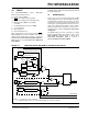
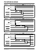
FIGURE 4-2: EXTERNAL POWER-ON
RESET CIRCUIT (FOR
SLOW V
DD POWER-UP)
Note 1: External Power-on Reset circuit is required
only if the V
DD power-up slope is too slow.
The diode D helps discharge the capacitor
quickly when V
DD powers down.
2: 15 k < R < 40 k is recommended to make
sure that the voltage drop across R does not
violate the device’s electrical specification.
3: R1 1 k will limit any current flowing into
MCLR
from external capacitor C, in the event
of MCLR
/VPP pin breakdown, due to
Electrostatic Discharge (ESD) or Electrical
Overstress (EOS).
C
R1
R
D
V
DD
MCLR
VDD
PIC
®
MCU