
Information


2010 Microchip Technology Inc. DS41303G-page 41
PIC18F2XK20/4XK20
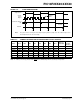
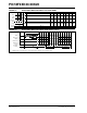
FIGURE 2-9: FSCM TIMING DIAGRAM
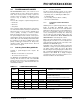
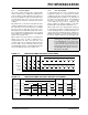
TABLE 2-3: SUMMARY OF REGISTERS ASSOCIATED WITH CLOCK SOURCES
OSCFIF
System
Clock
Output
Sample Clock
Failure
Detected
Oscillator
Failure
Note: The system clock is normally at a much higher frequency than the sample clock. The relative frequencies in
this example have been chosen for clarity.
(Q)
Test
Test Test
Clock Monitor Output
Name Bit 7 Bit 6 Bit 5 Bit 4 Bit 3 Bit 2 Bit 1 Bit 0
Value on
POR, BOR
Value on
all other
Resets
(1)
CONFIG1H IESO FCMEN — — FOSC3 FOSC2 FOSC1 FOSC0 — —
INTCON GIE/GIEH PEIE/GIEL
TMR0IE INT0IE RBIE TMR0IF INT0IF RBIF 0000 000x 0000 000x
OSCCON IDLEN IRCF2 IRCF1 IRCF0 OSTS IOFS SCS1 SCS0 0011 q000 0011 q000
OSCTUNE INTSRC PLLEN TUN5 TUN4 TUN3 TUN2 TUN1 TUN0 0000 0000 000u uuuu
PIE2 OSCFIE
C1IE C2IE EEIE BCLIE HLVDIE TMR3IE CCP2IE 0000 0000 0000 0000
PIR2 OSCFIF
C1IF C2IF EEIF BCLIF HLVDIF TMR3IF CCP2IF 0000 0000 0000 0000
IPR2 OSCFIP
— — — — — — — 1111 1111 1111 1111
Legend: x = unknown, u = unchanged, – = unimplemented locations read as ‘0’. Shaded cells are not used by oscillators.
Note 1: Other (non Power-up) Resets include MCLR
Reset and Watchdog Timer Reset during normal operation.