
Information


2010 Microchip Technology Inc. DS41303G-page 383
PIC18F2XK20/4XK20
26.12 AC (Timing) Characteristics
26.12.1 TIMING PARAMETER SYMBOLOGY
The timing parameter symbols have been created
using one of the following formats:
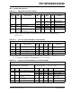
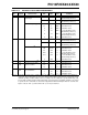
1. TppS2ppS 3. T
CC:ST (I
2
C™ specifications only)
2. TppS 4. Ts (I
2
C specifications only)
T
F Frequency T Time
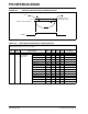
Lowercase letters (pp) and their meanings:
pp
cc CCP1 osc OSC1
ck CLKOUT rd RD
cs CS rw RD or WR
di SDI sc SCK
do SDO ss SS
dt Data in t0 T0CKI
io I/O port t1 T13CKI
mc MCLR
wr WR
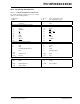
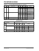
Uppercase letters and their meanings:
S
F Fall P Period
HHigh RRise
I Invalid (High-impedance) V Valid
L Low Z High-impedance
I
2
C only
AA output access High High
BUF Bus free Low Low
T
CC:ST (I
2
C specifications only)
CC
HD Hold SU Setup
ST
DAT DATA input hold STO Stop condition
STA Start condition