
Information


2010 Microchip Technology Inc. DS41303G-page 331
PIC18F2XK20/4XK20
CLRF Clear f
Syntax: CLRF f {,a}
Operands: 0 f 255
a [0,1]
Operation: 000h f
1 Z
Status Affected: Z
Encoding: 0110 101a ffff ffff
Description: Clears the contents of the specified
register.
If ‘a’ is ‘0’, the Access Bank is selected.
If ‘a’ is ‘1’, the BSR is used to select the
GPR bank.
If ‘a’ is ‘0’ and the extended instruction
set is enabled, this instruction operates
in Indexed Literal Offset Addressing
mode whenever f 95 (5Fh). See
Section 24.2.3 “Byte-Oriented and
Bit-Oriented Instructions in Indexed
Literal Offset Mode” for details.
Words: 1
Cycles: 1
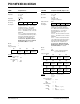
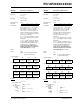
Q Cycle Activity:
Q1 Q2 Q3 Q4
Decode Read
register ‘f’
Process
Data
Write
register ‘f’
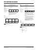
Example
: CLRF FLAG_REG, 1
Before Instruction
FLAG_REG = 5Ah
After Instruction
FLAG_REG = 00h
CLRWDT Clear Watchdog Timer
Syntax: CLRWDT
Operands: None
Operation: 000h WDT,
000h WDT postscaler,
1 TO,
1 PD
Status Affected: TO, PD
Encoding: 0000 0000 0000 0100
Description:
CLRWDT instruction resets the
Watchdog Timer. It also resets the
postscaler of the WDT. Status bits, TO
and PD
, are set.
Words: 1
Cycles: 1
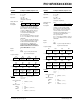
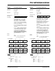
Q Cycle Activity:
Q1 Q2 Q3 Q4
Decode No
operation
Process
Data
No
operation
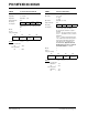
Example
: CLRWDT
Before Instruction
WDT Counter = ?
After Instruction
WDT Counter = 00h
WDT Postscaler = 0
TO
=1
PD
=1