
Information

PIC18F2XK20/4XK20
DS41303G-page 304 2010 Microchip Technology Inc.
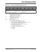
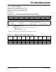
REGISTER 23-6: CONFIG5L: CONFIGURATION REGISTER 5 LOW
U-0 U-0 U-0 U-0 R/C-1 R/C-1 R/C-1
R/C-1
— — — —CP3
(1)
CP2
(1)
CP1
CP0
bit 7
bit 0
Legend:
R = Readable bit U = Unimplemented bit, read as ‘0’
-n = Value when device is unprogrammed C = Clearable only bit
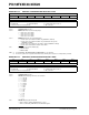
bit 7-4 Unimplemented: Read as ‘0’
bit 3 CP3: Code Protection bit
(1)
1 = Block 3 not code-protected
0 = Block 3 code-protected
bit 2 CP2: Code Protection bit
(1)
1 = Block 2 not code-protected
0 = Block 2 code-protected
bit 1 CP1: Code Protection bit
1 = Block 1 not code-protected
0 = Block 1 code-protected
bit 0 CP0: Code Protection bit
1 = Block 0 not code-protected
0 = Block 0 code-protected
Note 1: Implemented, but not used in PIC18FX3K20 and PIC18FX4K20 devices.
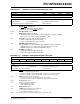
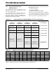
REGISTER 23-7: CONFIG5H: CONFIGURATION REGISTER 5 HIGH
R/C-1 R/C-1 U-0 U-0 U-0 U-0 U-0
U-0
CPD CPB — — — — —
—
bit 7
bit 0
Legend:
R = Readable bit U = Unimplemented bit, read as ‘0’
-n = Value when device is unprogrammed C = Clearable only bit
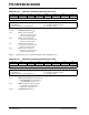
bit 7 CPD: Data EEPROM Code Protection bit
1 = Data EEPROM not code-protected
0 = Data EEPROM code-protected
bit 6 CPB: Boot Block Code Protection bit
1 = Boot Block not code-protected
0 = Boot Block code-protected
bit 5-0 Unimplemented: Read as ‘0’