
Information


PIC18F2XK20/4XK20
DS41303G-page 284 2010 Microchip Technology Inc.
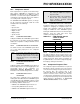
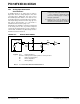
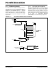
REGISTER 20-1: CM1CON0: COMPARATOR 1 CONTROL REGISTER 0
R/W-0 R-0 R/W-0 R/W-0 R/W-0 R/W-0 R/W-0 R/W-0
C1ON C1OUT C1OE C1POL C1SP C1R C1CH1 C1CH0
bit 7 bit 0
Legend:
R = Readable bit W = Writable bit U = Unimplemented bit, read as ‘0’
-n = Value at POR ‘1’ = Bit is set ‘0’ = Bit is cleared x = Bit is unknown
bit 7 C1ON: Comparator C1 Enable bit
1 = Comparator C1 is enabled
0 = Comparator C1 is disabled
bit 6 C1OUT: Comparator C1 Output bit
If C1POL =
1 (inverted polarity):
C1OUT = 0 when C1VIN+ > C1VIN-
C1OUT = 1 when C1V
IN+ < C1VIN-
If C1POL =
0 (non-inverted polarity):
C1OUT = 1 when C1VIN+ > C1VIN-
C1OUT = 0 when C1V
IN+ < C1VIN-
bit 5 C1OE: Comparator C1 Output Enable bit
1 = C1OUT is present on the C1OUT pin
(1)
0 = C1OUT is internal only
bit 4 C1POL: Comparator C1 Output Polarity Select bit
1 = C1OUT logic is inverted
0 = C1OUT logic is not inverted
bit 3 C1SP: Comparator C1 Speed/Power Select bit
1 = C1 operates in normal power, higher speed mode
0 = C1 operates in low-power, low-speed mode
bit 2 C1R: Comparator C1 Reference Select bit (non-inverting input)
1 = C1V
IN+ connects to C1VREF output
0 = C1V
IN+ connects to C1IN+ pin
bit 1-0 C1CH<1:0>: Comparator C1 Channel Select bit
00 = C12IN0- pin of C1 connects to C1V
IN-
01 = C12IN1- pin of C1 connects to C1V
IN-
10 = C12IN2- pin of C1 connects to C1V
IN-
11 = C12IN3- pin of C1 connects to C1V
IN-
Note 1: Comparator output requires the following three conditions: C1OE = 1, C1ON = 1 and corresponding port
TRIS bit = 0.