
Information

2010 Microchip Technology Inc. DS41303G-page 277
PIC18F2XK20/4XK20
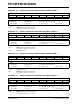
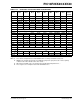
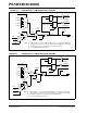
TABLE 19-2: REGISTERS ASSOCIATED WITH A/D OPERATION
Name Bit 7 Bit 6 Bit 5 Bit 4 Bit 3 Bit 2 Bit 1 Bit 0
Reset
Values
on page
INTCON GIE/GIEH PEIE/GIEL TMR0IE INT0IE RBIE TMR0IF INT0IF RBIF 59
PIR1 PSPIF
(1)
ADIF RCIF TXIF SSPIF CCP1IF TMR2IF TMR1IF 62
PIE1 PSPIE
(1)
ADIE RCIE TXIE SSPIE CCP1IE TMR2IE TMR1IE 62
IPR1
PSPIP
(1)
ADIP RCIP TXIP SSPIP CCP1IP TMR2IP TMR1IP 62
PIR2 OSCFIF C1IF C2IF EEIF BCLIF HLVDIF TMR3IF CCP2IF 62
PIE2 OSCFIE C1IE C2IE EEIE BCLIE HLVDIE TMR3IE CCP2IE 62
IPR2
OSCFIP C1IP C2IP EEIP BCLIP HLVDIP TMR3IP CCP2IP 62
ADRESH A/D Result Register, High Byte 61
ADRESL A/D Result Register, Low Byte 61
ADCON0
— — CHS3 CHS2 CHS1 CHS0 GO/DONE ADON 61
ADCON1
— —VCFG1VCFG0— — — —61
ADCON2 ADFM
— ACQT2 ACQT1 ACQT0 ADCS2 ADCS1 ADCS0 61
ANSEL ANS7
(1)
ANS6
(1)
ANS5
(1)
ANS4 ANS3 ANS2 ANS1 ANS0 62
ANSELH
— — — ANS12 ANS11 ANS10 ANS9 ANS8 62
PORTA RA7
(2)
RA6
(2)
RA5 RA4 RA3 RA2 RA1 RA0 62
TRISA TRISA7
(2)
TRISA6
(2)
PORTA Data Direction Control Register 62
PORTB RB7 RB6 RB5 RB4 RB3 RB2 RB1 RB0 62
TRISB PORTB Data Direction Control Register 62
LATB PORTB Data Latch Register (Read and Write to Data Latch) 62
PORTE
(4)
— — — —RE3
(3)
RE2 RE1 RE0 62
TRISE
(4)
IBF OBF IBOV PSPMODE — TRISE2 TRISE1 TRISE0 62
LATE
(4)
— — — — — PORTE Data Latch Register 62
Legend: — = unimplemented, read as ‘0’. Shaded cells are not used for A/D conversion.
Note 1: These bits are unimplemented on PIC18F2XK20 devices; always maintain these bits clear.
2: PORTA<7:6> and their direction bits are individually configured as port pins based on various primary
oscillator modes. When disabled, these bits read as ‘0’.
3: RE3 port bit is available only as an input pin when the MCLRE Configuration bit is ‘0’.
4: These registers are not implemented on PIC18F2XK20 devices.