
Information


2010 Microchip Technology Inc. DS41303G-page 271
PIC18F2XK20/4XK20
19.2.10 ADC REGISTER DEFINITIONS
The following registers are used to control the opera-
tion of the ADC.
Note: Analog pin control is performed by the
ANSEL and ANSELH registers. For ANSEL
and ANSELH registers, see Register 10-2
and Register 10-3, respectively.
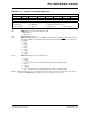
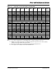
REGISTER 19-1: ADCON0: A/D CONTROL REGISTER 0
U-0 U-0 R/W-0 R/W-0 R/W-0 R/W-0 R/W-0 R/W-0
— — CHS3 CHS2 CHS1 CHS0 GO/DONE ADON
bit 7 bit 0
Legend:
R = Readable bit W = Writable bit U = Unimplemented bit, read as ‘0’
-n = Value at POR ‘1’ = Bit is set ‘0’ = Bit is cleared x = Bit is unknown
bit 7-6 Unimplemented: Read as ‘0’
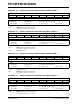
bit 5-2 CHS<3:0>: Analog Channel Select bits
0000 = AN0
0001 = AN1
0010 = AN2
0011 = AN3
0100 = AN4
0101 = AN5
(1)
0110 = AN6
(1)
0111 = AN7
(1)
1000 = AN8
1001 = AN9
1010 = AN10
1011 = AN11
1100 = AN12
1101 = Reserved
1110 = Reserved
1111 = FVR (1.2 Volt Fixed Voltage Reference)
(2)
bit 1 GO/DONE: A/D Conversion Status bit
1 = A/D conversion cycle in progress. Setting this bit starts an A/D conversion cycle.
This bit is automatically cleared by hardware when the A/D conversion has completed.
0 = A/D conversion completed/not in progress
bit 0 ADON: ADC Enable bit
1 = ADC is enabled
0 = ADC is disabled and consumes no operating current
Note 1: These channels are not implemented on PIC18F2XK20 devices.
2: Allow greater than 15 s acquisition time when measuring the Fixed Voltage Reference.