
Information


2010 Microchip Technology Inc. DS41303G-page 25
PIC18F2XK20/4XK20
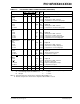
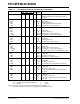
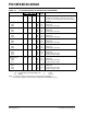
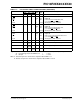
PORTE is a bidirectional I/O port
RE0/RD
/AN5
RE0
RD
AN5
82525
I/O
I
I
ST
TTL
Analog
Digital I/O
Read control for Parallel Slave Port
(see related WR
and CS pins)
Analog input 5, ADC channel 5
RE1/WR/AN6
RE1
WR
AN6
92626
I/O
I
I
ST
TTL
Analog
Digital I/O
Write control for Parallel Slave Port
(see related CS
and RD pins)
Analog input 6, ADC channel 6
RE2/CS/AN7
RE2
CS
AN7
10 27 27
I/O
I
I
ST
TTL
Analog
Digital I/O
Chip Select control for Parallel Slave Port
(see related RD
and WR)
Analog input 7, ADC channel 7
RE3 — — — — — See MCLR
/VPP/RE3 pin
VSS 12, 31 6, 30,
31
6, 29 P — Ground reference for logic and I/O pins
V
DD 11, 32 7, 8,
28, 29
7, 28 P — Positive supply for logic and I/O pins
NC — 13 12, 13,
33, 34
— — No connect
TABLE 1-3: PIC18F4XK20 PINOUT I/O DESCRIPTIONS (CONTINUED)
Pin Name
Pin Number
Pin
Type
Buffer
Type
Description
PDIP QFN TQFP
Legend: TTL = TTL compatible input CMOS = CMOS compatible input or output
ST = Schmitt Trigger input with CMOS levels I = Input
O = Output P = Power
Note 1: Default assignment for CCP2 when Configuration bit CCP2MX is set.
2: Alternate assignment for CCP2 when Configuration bit CCP2MX is cleared.