
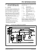
Information


2010 Microchip Technology Inc. DS41303G-page 23
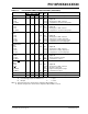
PIC18F2XK20/4XK20
PORTC is a bidirectional I/O port.
RC0/T1OSO/T13CKI
RC0
T1OSO
T13CKI
15 34 32
I/O
O
I
ST
—
ST
Digital I/O
Timer1 oscillator output
Timer1/Timer3 external clock input
RC1/T1OSI/CCP2
RC1
T1OSI
CCP2
(1)
16 35 35
I/O
I
I/O
ST
CMOS
ST
Digital I/O
Timer1 oscillator input
Capture 2 input/Compare 2 output/PWM 2 output
RC2/CCP1/P1A
RC2
CCP1
P1A
17 36 36
I/O
I/O
O
ST
ST
—
Digital I/O
Capture 1 input/Compare 1 output/PWM 1 output
Enhanced CCP1 output
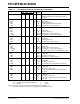
RC3/SCK/SCL
RC3
SCK
SCL
18 37 37
I/O
I/O
I/O
ST
ST
ST
Digital I/O
Synchronous serial clock input/output for
SPI mode
Synchronous serial clock input/output for I
2
C™ mode
RC4/SDI/SDA
RC4
SDI
SDA
23 42 42
I/O
I
I/O
ST
ST
ST
Digital I/O
SPI data in
I
2
C™ data I/O
RC5/SDO
RC5
SDO
24 43 43
I/O
O
ST
—
Digital I/O
SPI data out
RC6/TX/CK
RC6
TX
CK
25 44 44
I/O
O
I/O
ST
—
ST
Digital I/O
EUSART asynchronous transmit
EUSART synchronous clock (see related RX/DT)
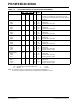
RC7/RX/DT
RC7
RX
DT
26 1 1
I/O
I
I/O
ST
ST
ST
Digital I/O
EUSART asynchronous receive
EUSART synchronous data (see related TX/CK)
TABLE 1-3: PIC18F4XK20 PINOUT I/O DESCRIPTIONS (CONTINUED)
Pin Name
Pin Number
Pin
Type
Buffer
Type
Description
PDIP QFN TQFP
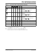
Legend: TTL = TTL compatible input CMOS = CMOS compatible input or output
ST = Schmitt Trigger input with CMOS levels I = Input
O = Output P = Power
Note 1: Default assignment for CCP2 when Configuration bit CCP2MX is set.
2: Alternate assignment for CCP2 when Configuration bit CCP2MX is cleared.