
Information


2010 Microchip Technology Inc. DS41303G-page 201
PIC18F2XK20/4XK20
17.3.8 OPERATION IN POWER-MANAGED
MODES
In SPI Master mode, module clocks may be operating
at a different speed than when in full power mode; in
the case of the Sleep mode, all clocks are halted.
In all Idle modes, a clock is provided to the peripherals.
That clock could be from the primary clock source, the
secondary clock (Timer1 oscillator at 32.768 kHz) or
the INTOSC source. See Section 3.0 “Power-Man-
aged Modes” for additional information.
In most cases, the speed that the master clocks SPI
data is not important; however, this should be
evaluated for each system.
When MSSP interrupts are enabled, after the master
completes sending data, an MSSP interrupt will wake
the controller:
• from Sleep, in slave mode
• from Idle, in slave or master mode
If an exit from Sleep or Idle mode is not desired, MSSP
interrupts should be disabled.
In SPI master mode, when the Sleep mode is selected,
all module clocks are halted and the transmis-
sion/reception will remain in that state until the devices
wakes. After the device returns to Run mode, the mod-
ule will resume transmitting and receiving data.
In SPI Slave mode, the SPI Transmit/Receive Shift
register operates asynchronously to the device. This
allows the device to be placed in any power-managed
mode and data to be shifted into the SPI
Transmit/Receive Shift register. When all 8 bits have
been received, the MSSP interrupt flag bit will be set
and if enabled, will wake the device.
17.3.9 EFFECTS OF A RESET
A Reset disables the MSSP module and terminates the
current transfer.
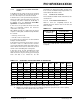
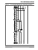
17.3.10 BUS MODE COMPATIBILITY
Table 17-1 shows the compatibility between the
standard SPI modes and the states of the CKP and
CKE control bits.
TABLE 17-1: SPI BUS MODES
There is also an SMP bit which controls when the data
is sampled.
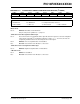
TABLE 17-2: REGISTERS ASSOCIATED WITH SPI OPERATION
Standard SPI Mode
Terminology
Control Bits State
CKP CKE
0, 0 0 1
0, 1 0 0
1, 0 1 1
1, 1 1 0
Name Bit 7 Bit 6 Bit 5 Bit 4 Bit 3 Bit 2 Bit 1 Bit 0
Reset
Values
on page
INTCON GIE/GIEH PEIE/GIEL
TMR0IE INT0IE RBIE TMR0IF INT0IF RBIF 59
PIR1
PSPIF
(1)
ADIF RCIF TXIF SSPIF CCP1IF TMR2IF TMR1IF 62
PIE1
PSPIE
(1)
ADIE RCIE TXIE SSPIE CCP1IE TMR2IE TMR1IE 62
IPR1 PSPIP
(1)
ADIP RCIP TXIP SSPIP CCP1IP TMR2IP TMR1IP 62
TRISA
TRISA7
(2)
TRISA6
(2)
TRISA5 TRISA4 TRISA3 TRISA2 TRISA1 TRISA0 62
TRISC
TRISC7 TRISC6 TRISC5 TRISC4 TRISC3 TRISC2 TRISC1 TRISC0 62
SSPBUF SSP Receive Buffer/Transmit Register 60
SSPCON1 WCOL SSPOV SSPEN CKP SSPM3 SSPM2 SSPM1 SSPM0 60
SSPSTAT SMP CKE
D/A P S R/W UA BF 60
Legend: Shaded cells are not used by the MSSP in SPI mode.
Note 1: These bits are unimplemented in 28-pin devices; always maintain these bits clear.
2: PORTA<7:6> and their direction bits are individually configured as port pins based on various primary
oscillator modes. When disabled, these bits read as ‘0’.