
Information

PIC18F2XK20/4XK20
DS41303G-page 176 2010 Microchip Technology Inc.
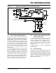
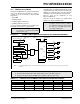
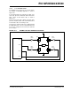
FIGURE 16-2: EXAMPLE PWM (ENHANCED MODE) OUTPUT RELATIONSHIPS (ACTIVE-HIGH
STATE)
0
Period
00
10
01
11
Signal
PR2+1
P1M<1:0>
P1A Modulated
P1A Modulated
P1B Modulated
P1A Active
P1B Inactive
P1C Inactive
P1D Modulated
P1A Inactive
P1B Modulated
P1C Active
P1D Inactive
Pulse
Width
(Single Output)
(Half-Bridge)
(Full-Bridge,
Forward)
(Full-Bridge,
Reverse)
Delay
(1)
Delay
(1)
Relationships:
• Period = 4 * T
OSC * (PR2 + 1) * (TMR2 Prescale Value)
• Pulse Width = T
OSC * (CCPR1L<7:0>:CCP1CON<5:4>) * (TMR2 Prescale Value)
• Delay = 4 * T
OSC * (PWM1CON<6:0>)
Note 1: Dead-band delay is programmed using the PWM1CON register (Section 16.4.6 “Programmable Dead-Band Delay
mode”).