
Information


PIC18F2XK20/4XK20
DS41303G-page 168 2010 Microchip Technology Inc.
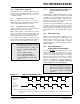
14.2 Timer2 Interrupt
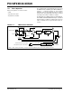
Timer2 can also generate an optional device interrupt.
The Timer2 output signal (TMR2-to-PR2 match) pro-
vides the input for the 4-bit output counter/postscaler.
This counter generates the TMR2 match interrupt flag
which is latched in TMR2IF of the PIR1 register. The
interrupt is enabled by setting the TMR2 Match Inter-
rupt Enable bit, TMR2IE of the PIE1 register.
A range of 16 postscale options (from 1:1 through 1:16
inclusive) can be selected with the postscaler control
bits, T2OUTPS<3:0> of the T2CON register.
14.3 Timer2 Output
The unscaled output of TMR2 is available primarily to
the CCP modules, where it is used as a time base for
operations in PWM mode.
Timer2 can be optionally used as the shift clock source
for the MSSP module operating in SPI mode. Addi-
tional information is provided in Section 17.0 “Master
Synchronous Serial Port (MSSP) Module”.
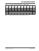
FIGURE 14-1: TIMER2 BLOCK DIAGRAM
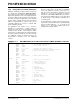
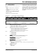
TABLE 14-1: REGISTERS ASSOCIATED WITH TIMER2 AS A TIMER/COUNTER
Name Bit 7 Bit 6 Bit 5 Bit 4 Bit 3 Bit 2 Bit 1 Bit 0
Reset
Values
on page
INTCON GIE/GIEH PEIE/GIEL TMR0IE INT0IE RBIE TMR0IF INT0IF RBIF 59
PIR1
PSPIF
(1)
ADIF RCIF TXIF SSPIF CCP1IF TMR2IF TMR1IF 62
PIE1 PSPIE
(1)
ADIE RCIE TXIE SSPIE CCP1IE TMR2IE TMR1IE 62
IPR1 PSPIP
(1)
ADIP RCIP TXIP SSPIP CCP1IP TMR2IP TMR1IP 62
TMR2 Timer2 Register 60
T2CON
— T2OUTPS3 T2OUTPS2 T2OUTPS1 T2OUTPS0 TMR2ON T2CKPS1 T2CKPS0 60
PR2 Timer2 Period Register 60
Legend: — = unimplemented, read as ‘0’. Shaded cells are not used by the Timer2 module.
Note 1: These bits are unimplemented on 28-pin devices; always maintain these bits clear.
Comparator
TMR2 Output
TMR2
Postscaler
Prescaler
PR2
2
F
OSC/4
1:1 to 1:16
1:1, 1:4, 1:16
4
T2OUTPS<3:0>
T2CKPS<1:0>
Set TMR2IF
Internal Data Bus
8
Reset
TMR2/PR2
8
8
(to PWM or MSSP)
Match