
Information


2010 Microchip Technology Inc. DS41303G-page 139
PIC18F2XK20/4XK20
10.9 Parallel Slave Port
In addition to its function as a general I/O port, PORTD
can also operate as an 8-bit wide Parallel Slave Port
(PSP) or microprocessor port. PSP operation is
controlled by the 4 upper bits of the TRISE register
(Register 10-1). Setting control bit, PSPMODE
(TRISE<4>), enables PSP operation as long as the
enhanced CCP module is not operating in dual output
or quad output PWM mode. In Slave mode, the port is
asynchronously readable and writable by the external
world.
The PSP can directly interface to an 8-bit
microprocessor data bus. The external microprocessor
can read or write the PORTD latch as an 8-bit latch.
Setting the control bit, PSPMODE, enables the PORTE
I/O pins to become control inputs for the microprocessor
port. When set, port pin RE0 is the RD
input, RE1 is the
WR
input and RE2 is the CS (Chip Select) input. For this
functionality, the corresponding data direction bits of the
TRISE register (TRISE<2:0>) must be configured as
inputs (set) and the ANSEL<7:5> bits must be cleared.
A write to the PSP occurs when both the CS
and WR
lines are first detected low and ends when either are
detected high. The PSPIF and IBF flag bits are both set
when the write ends.
A read from the PSP occurs when both the CS
and RD
lines are first detected low. The data in PORTD is read
out and the OBF bit is clear. If the user writes new data
to PORTD to set OBF, the data is immediately read out;
however, the OBF bit is not set.
When either the CS
or RD lines are detected high, the
PORTD pins return to the input state and the PSPIF bit
is set. User applications should wait for PSPIF to be set
before servicing the PSP; when this happens, the IBF
and OBF bits can be polled and the appropriate action
taken.
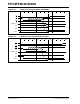
The timing for the control signals in Write and Read
modes is shown in Figure 10-3 and Figure 10-4,
respectively.
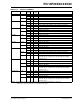
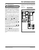
FIGURE 10-2: PORTD AND PORTE
BLOCK DIAGRAM
(PARALLEL SLAVE PORT)
Note: The Parallel Slave Port is only available on
PIC18F4XK20 devices.
Data Bus
WR LATD
RDx pin
QD
CK
EN
QD
EN
RD PORTD
One bit of PORTD
Set Interrupt Flag
PSPIF (PIR1<7>)
Read
Chip Select
Write
RD
CS
WR
TTL
TTL
TTL
TTL
or
WR PORTD
RD LATD
Data Latch
Note: I/O pins have diode protection to VDD and VSS.
PORTE Pins