
Information


2010 Microchip Technology Inc. DS41303G-page 135
PIC18F2XK20/4XK20
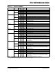
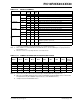
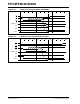
TABLE 10-9: PORTE I/O SUMMARY
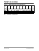
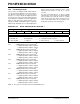
TABLE 10-10: SUMMARY OF REGISTERS ASSOCIATED WITH PORTE
Pin Function
TRIS
Setting
I/O
I/O
Type
Description
RE0/RD
/AN5 RE0 0 O DIG LATE<0> data output; not affected by analog input.
1 I ST PORTE<0> data input; disabled when analog input enabled.
RD
1 I TTL PSP read enable input (PSP enabled).
AN5 1 I ANA A/D input channel 5; default input configuration on POR.
RE1/WR
/AN6 RE1 0 O DIG LATE<1> data output; not affected by analog input.
1 I ST PORTE<1> data input; disabled when analog input enabled.
WR
1 I TTL PSP write enable input (PSP enabled).
AN6 1 I ANA A/D input channel 6; default input configuration on POR.
RE2/CS
/AN7 RE2 0 O DIG LATE<2> data output; not affected by analog input.
1 I ST PORTE<2> data input; disabled when analog input enabled.
CS
1 I TTL PSP write enable input (PSP enabled).
AN7 1 I ANA A/D input channel 7; default input configuration on POR.
MCLR/
VPP/
RE3
(1,2)
MCLR — I ST External Master Clear input; enabled when MCLRE Configuration bit is
set.
V
PP — I ANA High-voltage detection; used for ICSP™ mode entry detection. Always
available, regardless of pin mode.
RE3 —
(2)
I ST PORTE<3> data input; enabled when MCLRE Configuration bit is
clear.
Legend: DIG = Digital level output; TTL = TTL input buffer; ST = Schmitt Trigger input buffer; ANA = Analog level input/output;
x = Don’t care (TRIS bit does not affect port direction or is overridden for this option).
Note 1: RE3 is available on both PIC18F2XK20 and PIC18F4XK20 devices. All other PORTE pins are only implemented on
PIC18F4XK20 devices.
2: RE3 does not have a corresponding TRIS bit to control data direction.
Name Bit 7 Bit 6 Bit 5 Bit 4 Bit 3 Bit 2 Bit 1 Bit 0
Reset
Values
on page
PORTE
— — — —RE3
(1,2)
RE2 RE1 RE0 62
LATE
(2)
— — — — — LATE Data Output Register 62
TRISE
(3)
IBF OBF IBOV PSPMODE — TRISE2 TRISE1 TRISE0 62
SLRCON — — —SLRE
(3)
SLRD
(3)
SLRC SLRB SLRA 63
ANSEL ANS7
(3)
ANS6
(3)
ANS5
(3)
ANS4 ANS3 ANS2 ANS1 ANS0 62
Legend: — = unimplemented, read as ‘0’. Shaded cells are not used by PORTE.
Note 1: Implemented only when Master Clear functionality is disabled (MCLRE Configuration bit = 0).
2: RE3 is the only PORTE bit implemented on both PIC18F2XK20 and PIC18F4XK20 devices. All other bits
are implemented only when PORTE is implemented (i.e., PIC18F4XK20 devices).
3: Unimplemented on PIC18F2XK20 devices.