
Information


PIC18F2XK20/4XK20
DS41303G-page 102 2010 Microchip Technology Inc.
7.6 Operation During Code-Protect
Data EEPROM memory has its own code-protect bits
in Configuration Words. External read and write
operations are disabled if code protection is enabled.
The microcontroller itself can both read and write to the
internal data EEPROM, regardless of the state of the
code-protect Configuration bit. Refer to Section 23.0
“Special Features of the CPU” for additional
information.
7.7 Protection Against Spurious Write
There are conditions when the user may not want to
write to the data EEPROM memory. To protect against
spurious EEPROM writes, various mechanisms have
been implemented. On power-up, the WREN bit is
cleared. In addition, writes to the EEPROM are blocked
during the Power-up Timer period (T
PWRT,
parameter 33).
The write initiate sequence and the WREN bit together
help prevent an accidental write during brown-out,
power glitch or software malfunction.
7.8 Using the Data EEPROM
The data EEPROM is a high-endurance, byte
addressable array that has been optimized for the
storage of frequently changing information (e.g.,
program variables or other data that are updated often).
When variables in one section change frequently, while
variables in another section do not change, it is possible
to exceed the total number of write cycles to the
EEPROM (specification D124) without exceeding the
total number of write cycles to a single byte (specification
D120). If this is the case, then an array refresh must be
performed. For this reason, variables that change
infrequently (such as constants, IDs, calibration, etc.)
should be stored in Flash program memory.
A simple data EEPROM refresh routine is shown in
Example 7-3.
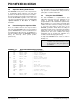
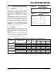
EXAMPLE 7-3: DATA EEPROM REFRESH ROUTINE
Note: If data EEPROM is only used to store
constants and/or data that changes rarely,
an array refresh is likely not required. See
specification.
CLRF EEADR ; Start at address 0
BCF EECON1, CFGS ; Set for memory
BCF EECON1, EEPGD ; Set for Data EEPROM
BCF INTCON, GIE ; Disable interrupts
BSF EECON1, WREN ; Enable writes
Loop ; Loop to refresh array
BSF EECON1, RD ; Read current address
MOVLW 55h ;
MOVWF EECON2 ; Write 55h
MOVLW 0AAh ;
MOVWF EECON2 ; Write 0AAh
BSF EECON1, WR ; Set WR bit to begin write
BTFSC EECON1, WR ; Wait for write to complete
BRA $-2
INCFSZ EEADR, F ; Increment address
BRA LOOP ; Not zero, do it again
BCF EECON1, WREN ; Disable writes
BSF INTCON, GIE ; Enable interrupts