
Information


2010 Microchip Technology Inc. DS80506C-page 9
PIC18F47J53 FAMILY
5. Module: Electrical Characteristics
Table 31-7 has been corrected and changes are shown
in bold below:
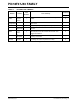
TABLE 31-7 USB MODULE SPECIFICATIONS
Operating Conditions: -40°C < TA < +85°C (unless otherwise stated)
Param
No.
Sym Characteristics Min Typ Max Units Comments
D313 V
USB USB Voltage 3.0 — 3.6 V Voltage on VUSB pin must
be in this range for proper
USB operation
D314 I
IL Input Leakage on D+ or D- — ±.075 +0.5 AVSS < VPIN < VUSB
D315 VILUSB Input Low Voltage for
USB Buffer
——0.8VFor VUSB range
D316 V
IHUSB Input High Voltage for
USB Buffer
2.0 — — V For VUSB range
D318 V
DIFS Differential Input Sensitivity — — 0.2 V The difference between D+
and D- must exceed this
value while VCM is met
D319 VCM Differential Common Mode
Range
0.8 — 2.5 V
D320 Z
OUT Driver Output Impedance
(1)
28 — 44
D321 VOL Voltage Output Low 0.0 — 0.3 V 1.5 kload connected to
3.6V
D322 V
OH Voltage Output High 2.8 — 3.6 V 1.5 kload connected to
ground
Note 1: The D+ and D- signal lines have built-in impedance matching resistors. No external resistors, capacitors or
magnetic components are necessary on the D+/D- signal paths between the PIC18F47J53 family device
and a USB cable.