
Information


PIC18F47J53 FAMILY
DS80506C-page 2 2010 Microchip Technology Inc.
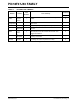
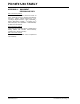
TABLE 2: SILICON ISSUE SUMMARY
Module Feature
Item
Number
Issue Summary
Affected
Revisions
(1)
A1
CTMU
Constant
Current
Source
1.
Band gap must be manually enabled before using the
CTMU. X
Oscillator
Configurations
PLL 2.
PLL can not be enabled unless the 8 or 4 MHz INTOSC
option is set.
X
ADC A/D 3. ANx pin may output a pull-up pulse during acquisition. X
EUSART
Receive
Baud Rate
4.
Receive and transmit baud rates differ due to different clock
sources.
X
MSSP
I
2
C™
Mode
5.
If a Stop condition occurs in the middle of an address or
data reception, there will be issues with the SCL clock
stream and RCEN bit.
X
MSSP
I
2
C Slave
Reception
6.
In I
2
C slave reception, the module may have problems
receiving correct data.
X
EUSART
Enable/
Disable
7.
If interrupts are enabled, disabling and
re-enabling the module requires a 2 T
CY delay.
X
Note 1: Only those issues indicated in the last column apply to the current silicon revision.