
Information


PIC18F24K20/25K20/44K20/45K20
DS80000425K-page 8 2008-2013 Microchip Technology Inc.
25. Module: Configuration Bits
Bit 3 of CONFIG3H defaults to ‘0’ after a Bulk
Erase instead of ‘1’ as specified in the data sheet.
Work around
Program the HFOFST bit to the desired state after
a Bulk Erase. All MPLAB
®
IDE programming tools
currently perform this way.
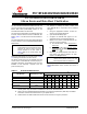
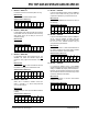
Affected Silicon Revisions
26. Module: EUSART
In Asynchronous Receive mode, the RCIDL bit of
the BAUDCON register will properly go low when
an invalid Start bit less than 1/8th of a bit time is
received. The RCIDL bit will then stay low improp-
erly until a valid Start bit is received.
Work around
When monitoring the RCIDL bit, measure the
length of time between the RCIDL going low and
the RCIF flag going high. If this time is greater than
one character time, then restore the RCIDL bit by
resetting the EUSART module. The EUSART
module is reset when the SPEN bit of the RCSTA
register is cleared.
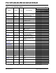
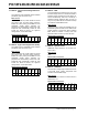
Affected Silicon Revisions
27. Module: PORTB
Setting a PORTB interrupt-on-change enable bit of
the IOCB register while the corresponding PORTB
input is high will cause an RBIF interrupt.
Work around
Set the IOCB bits to the desired configuration, then
read PORTB to clear the mismatch latches.
Finally, clear the RBIF bit before setting the RBIE
bit.
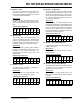
Affected Silicon Revisions
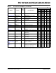
28. Module: ADC
After extended stress, the Most Significant bit
(MSb) of the ADC conversion result can become
stuck at ‘0’. Conversions resulting in code 511 or
less are still accurate, but conversions that should
result in codes greater than 511 are, instead,
pinned at 511.
The potential for failures is a function of several
factors:
• The potential for failures increases over the life
of the part. No failures have ever been seen for
accelerated stress estimated to be equivalent
to 34 years at room temperature. The failure
rate after accelerated stress estimated to be
equivalent to 146 years at room temperature
can be as high as 10% for V
DD = 1.8V. The time
to failure will decrease as the operating
temperature increases.
• The potential for failures is highest at low V
DD
and decreases as V
DD increases.
Work around
1. Restrict the input voltage to less than 1/2 of the
ADC voltage reference so that the expected
result is always a code less than or equal to 511.
2. Use manual acquisition time (ACQT<2:0> =
000) and put the part to Sleep after each
conversion.
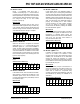
Affected Silicon Revisions
29. Module: ECCP
Changing direction in Full-Bridge mode inserts a
dead-band time of 4/F
OSC * TMR2 Prescale
instead of 1/F
OSC * TMR2 Prescale as specified in
the data sheet.
Work around
None.
Affected Silicon Revisions
0xA
0xC
0xE
0x11
0x16
0x18
0x19
0x1B
0x1C
XXXX
0xA
0xC
0xE
0x11
0x16
0x18
0x19
0x1B
0x1C
XXXX
0xA
0xC
0xE
0x11
0x16
0x18
0x19
0x1B
0x1C
XXXXXXXXX
0xA
0xC
0xE
0x11
0x16
0x18
0x19
0x1B
0x1C
XXXXXXX
0xA
0xC
0xE
0x11
0x16
0x18
0x19
0x1B
0x1C
XXXXX