
Datasheet
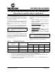

© 2009 Microchip Technology Inc. DS80366G-page 5
PIC18F24/25/44/45K20
15. Module: High Low Voltage Detect (HLVD)
The IVRST bit of the HLVDCON register activates
prematurely (Rev. A4 and A7 only).
Work around
Wait an additional 20 µs after IVRST is sensed
high before using the fixed voltage reference.
Enable the FVR by setting the FVREN bit of the
CVRCON2 register before activating any periph-
eral that automatically enables the FVR. Peripher-
als that automatically enable the FVR include the
Brown-out Reset, the High/Low Voltage Detect,
and the HFINTOSC.
Affected Silicon Revisions
16. Module: BOR
An unexpected Brown-out Reset may occur when
the fixed voltage reference is inactive and BOR is
activated, thereby activating the fixed voltage
reference simultaneously. This error is caused by
a premature FVRST stable flag (Rev. A4 and A7
only).
Work around
Enable the FVR by setting the FVREN bit of the
CVRCON2 register and then wait an additional
20 µs after FVRST is sensed high before
enabling BOR. Brown-out disable in Sleep mode
with automatic enable on wake-up cannot be used.
Affected Silicon Revisions
17. Module: System Clocks
HFINTOSC output frequency is 16 MHz ± 3%
25°C to 85°C.
Work around
None.
Affected Silicon Revisions
18. Module: POR/BOR
The POR rearm voltage may be below the low end
of the BOR range causing unexpected code
execution below the BOR range.
Work around
Use external power monitor to hold device in
Reset below 1.1 Volts.
Affected Silicon Revisions
19. Module: POR
The POR may release around 0.8 volts (below the
POR rearm voltage of 1.2V nominal) when V
DD
rises from below either 0.60V (when BOR is not
enabled) or 0.33V (when BOR is enabled).
Work around
Use Power-up Timer when operating with the EC,
EXTRC or HFINTOSC oscillator modes. Ensure that
VDD rise time is less than the Power-up Timer time.
Affected Silicon Revisions
20. Module: POR
The part may hang in the Reset state when VDD
rises to the operating range at a rate faster than
7500 volts per second. Recovery from the hung
state is possible only by first lowering VDD to below
0.3V followed by raising V
DD to the operating
range.
Work around
Slow VDD rise time by adding series resistance
between the voltage supply and the V
DD pin and
increasing the V
DD bypass capacitance. VDD
bypassing should remain on the pin side of the
series resistor.
Affected Silicon Revisions
A4 A7 A9 AB
XX
A4 A7 A9 AB
XX
A4 A7 A9 AB
XXX
X
A4 A7 A9 AB
XXX
X
A4 A7 A9
AB
XXX
X
A4 A7 A9
AB
XXX
X