
Information


2011 Microchip Technology Inc. DS80436D-page 7
PIC18F46J50 FAMILY
7. Module: DC Characteristics (Supply
Voltage)
The minimum operating voltage (VDD) parameter
(D001) for “F” devices is 2.25V. For “LF” devices
(such as the PIC18LF46J50), the minimum rated
V
DD operating voltage is 2.0V.
Work around
None.
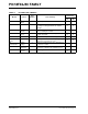
Affected Silicon Revisions
8. Module: Analog-to-Digital Converter
(Band Gap Reference)
At high VDD voltages (ex: >2.5V), performing an
ADC conversion on Channel 15 (the V
BG absolute
reference) can temporarily disturb the reference
voltage supplied to the HLVD module and compar-
ator module (only when configured to use the
VIRV). At lower VDD voltages, the disturbance will
be less or non-existent.
Work around
If precise HLVD or comparator VIRV thresholds are
required at high V
DD voltages, avoid performing
ADC conversions on Channel 15 while simultane-
ously using the HLVD or comparator V
IRV. If an
ADC conversion is performed on Channel 15, a
settling time of approximately 100 s is needed
before the reference voltage fully returns to the
original value.
Affected Silicon Revisions
9. Module: Charge Time Measurement Unit
(CTMU)
On an “F” device, the CTMU current source will stop
sourcing current if the applied V
DD voltage falls
below the LVDSTAT (WDTCON<6>) threshold
(2.45V nominal). When VDD is above the LVDSTAT
threshold, the CTMU will function normally. This
issue does not apply to “LF” devices. The current
source will continue to function normally at all rated
voltages for these devices.
Work around
None
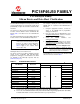
Affected Silicon Revisions
A2 A4
X
A2 A4
X
X
A2 A4
X