
Information


PIC18F46J50 FAMILY
DS80436D-page 2 2011 Microchip Technology Inc.
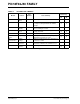
TABLE 2: SILICON ISSUE SUMMARY
Module Feature
Item
Number
Issue Summary
Affected
Revisions
(1)
A2 A4
MSSP I
2
C™
Modes
1. Must keep LATB<5:4> bits clear.
X
MSSP I
2
C Slave 2. Module may not receive the correct data if there
is a delay in reading SSPxBUF after SSPxIF
interrupt.
XX
EUSART Enable/
Disable
3. If interrupts are enabled, a 2 TCY delay needed
after re-enabling the module.
XX
A/D F
OSC/2
Clock
4. FOSC/2 A/D Conversion mode may not meet
linearity error limits.
XX
PMP PSP/PMP 5. The data bus may not work correctly. X
Low-Power
modes
Deep Sleep 6. Wake-up events that occur during Deep Sleep
entry may not generate an event.
XX
DC
Characteristics
Supply
Voltage
7. Minimum operating voltage (V
DD) parameter for
“F” devices is 2.25V.
X
A/D Band Gap
Reference
8. At high V
DD voltages, performing an A/D
conversion on Channel 15 could have issues.
XX
CTMU Constant
Current
9. Low voltages turn off constant current source.
X
Note 1: Only those issues indicated in the last column apply to the current silicon revision.