
Information

© 2007 Microchip Technology Inc. DS80283E-page 5
PIC18F2585/2680/4585/4680
19. Module: MSSP
It has been observed that following a Power-on
Reset, I
2
C mode may not initialize properly by just
configuring the SCL and SDA pins as either inputs
or outputs. This has only been seen in a few
unique system environments.
A test of a statistically significant sample of pre-
production systems, across the voltage and
current range of the application’s power supply,
should indicate if a system is susceptible to this
issue.
Work around
Before configuring the module for I
2
C operation:
1. Configure the SCL and SDA pins as outputs by
clearing their corresponding TRIS bits.
2. Force SCL and SDA low by clearing the
corresponding LAT bits.
3. While keeping the LAT bits clear, configure
SCL and SDA as inputs by setting their TRIS
bits.
Once this is done, use the SSPCON1 and
SSPCON2 registers to configure the proper I
2
C
mode as before.
Date Codes that pertain to this issue:
All engineering and production devices.
20. Module: MSSP
When the MSSP is configured for SPI mode, the
Buffer Full Status bit, BF (SSPSTAT<0>), should
not be polled in software to determine when the
transfer is complete.
Work around
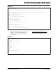
Copy the SSPSTAT register into a variable and
perform the bit test on the variable. In Example 2,
SSPSTAT is copied into the working register
where the bit test is performed.
EXAMPLE 2:
A second option is to poll the Master Synchronous
Serial Port Interrupt Flag bit, SSPIF (PIR1<3>).
This bit can be polled and will set when the transfer
is complete.
Date Codes that pertain to this issue:
All engineering and production devices.
21. Module: MSSP
In SPI mode, the SDO output may change after the
inactive clock edge of the bit ‘0’ output. This may
affect some SPI components that read data over
300 ns after the inactive edge of SCK.
Work around
None
Date Codes that pertain to this issue:
All engineering and production devices.
22. Module: DC Characteristics (BOR)
The values for parameter D005 (VBOR) in
Section 27.1 “DC Characteristics: Supply
Voltage” of the Device Data Sheet, when the trip
point for BORV1:BORV0 = 11, are not applicable
as the device may reset below the minimum
operating voltage for the device.
Work around
None.
Date Codes that pertain to this issue:
All engineering and production devices.
23. Module: BOD/HLVD
Due to production tolerances, selecting the lowest
setting for Brown-out Detect (BORV1:BORV0 = 11)
or Low-Voltage Reset (LVV = 0000) is not recom-
mended, since it may result in an actual Brown-out
Reset or Low-Voltage Detect below the minimum
allowable V
DD of 2.0V.
Work around
Use the next highest BOD or HLVD voltage thresh-
old to ensure a low V
DD is detected before it drops
below 2.0V.
Date Codes that pertain to this issue:
All engineering and production devices.
loop_MSB:
MOVF SSPSTAT, W
BTFSS WREG, BF
BRA loop_MSB