
Information

PIC18F2585/2680/4585/4680
DS80272B-page 4 © 2007 Microchip Technology Inc.
2. Module: ECAN™ Technology
The first paragraph of Section 23.6.1 “Initiating
Transmission” is modified as shown.
23.6.1 INITIATING TRANSMISSION
For the MCU to have write access to the message
buffer, the TXREQ bit must be clear, indicating that the
message buffer is clear of any pending message to be
transmitted.
At a minimum, the SIDH, SIDL and DLC registers must
be loaded. If data bytes are present in the message, the
data registers must also be loaded. If the message is to
use extended identifiers, the EIDH:EIDL registers must
also be loaded and the EXIDE bit set.
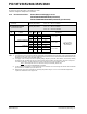
3. Module: Electrical Characteristics
A row is changed in Table 27-24. The new and
modified content is indicated by bold text.
TABLE 27-24: A/D CONVERTER CHARACTERISTICS:PIC18F2585/2680/4585/4680 (INDUSTRIAL)
PIC18LF2585/2680/4585/4680 (INDUSTRIAL)
Note: The time between the clearing of the
TXREQ bit and when the TX buffer has
write access can be as long as four
instruction cycles.
Param
No.
Sym Characteristic Min Typ Max Units Conditions
...
A04 E
DL Differential Linearity Error — — <±1 LSb ΔVREF ≥ 3.0V
A06 EOFF Offset Error — — <±2 LSb VREF = VSS and VDD
A07 EGN Gain Error — — <±1 LSb ΔVREF ≥ 3.0V
...
Note 1: The A/D conversion result never decreases with an increase in the input voltage and has no missing codes.
2: When A/D is off, it will not consume any current other than minor leakage current. The power-down current
spec includes any such leakage from the A/D module.
3: V
REFH current is from RA3/AN3/VREF+ pin or AVDD, whichever is selected as the VREFH source.
V
REFL current is from RA2/AN2/VREF- pin or AVSS, whichever is selected as the VREFL source.