
Information


© 2007 Microchip Technology Inc. DS80289E-page 1
PIC18F2423/2523/4423/4523
The PIC18F2423/2523/4423/4523 Rev. B2 parts you
have received conform functionally to the Device Data
Sheet (DS39755B), except for the anomalies
described below. Any Data Sheet Clarification issues
related to the PIC18F2423/2523/4423/4523 will be
reported in a separate Data Sheet errata. Please check
the Microchip web site for any existing issues.
The following silicon errata apply only to
PIC18F2423/2523/4423/4523 devices with these
Device/Revision IDs:
1. Module: MSSP
In SPI Slave mode with slave select enabled
(SSPM<3:0> = 0100), the minimum time between
the falling edge of the SS pin and first SCK edge
is greater than specified in parameter 70 in
Table 26-14 and Table 26-16. The updated
specification is shown in bold in Table 1.
The minimum time between SS
pin low and an
SSPBUF write is also 3 T
CY. If the falling edge of
the SS
pin occurs greater than 3 TCY before the
first SCK edge, or loading SSPBUF, the peripheral
will function correctly. Also, if SSPBUF is written
prior to the SS
pin going low, the peripheral will
function correctly.
Work around
None.
Date Codes that pertain to this issue:
All engineering and production devices.
TABLE 1: EXAMPLE SPI MODE REQUIREMENTS (SLAVE MODE TIMING)
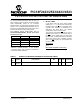
Part Number Device ID Revision ID
PIC18F2423 0001 0001 010 10101
PIC18F2523 0001 0001 000 10101
PIC18F4423 0001 0000 110 10101
PIC18F4523 0001 0000 100 10101
The Device IDs (DEVID1 and DEVID2) are located at
addresses 3FFFFEh:3FFFFFh in the device’s
configuration space. They are shown in hexadecimal
in the format “DEVID2 DEVID1”.
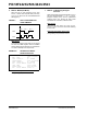
Param
No.
Symbol Characteristic Min Max Units Conditions
70 T
SSL2SCH,
T
SSL2SCL
SS
↓ to SCK ↓ or SCK ↑ Input 3TCY —ns
PIC18F2423/2523/4423/4523 Rev. B2 Silicon Errata