
Information


© 2007 Microchip Technology Inc. DS80199E-page 3
PIC18F2515/2610/4515/4610
8. Module: ECCP and CCP
The ECCP1 and CCP2 configured for PWM mode,
with 1:1 Timer2 prescaler and duty cycle set to the
period minus 1, may result in the PWM output(s)
remaining at a logic low level.
Clearing the PR2 register to select the fastest
period may also result in the output(s) remaining at
a logic low output level.
Work around
To ensure a reliable waveform, verify that the
selected duty cycle does not equal the 10-bit
period minus 1 prior to writing these locations, or
use 1:4 or 1:16 Timer2 prescale. Also, verify the
PR2 register is not written to 00h.
All other duty cycle and period settings will function
as described in the Device Data Sheet.
The ECCP and CCP modules remain capable of
10-bit accuracy.
Date Codes that pertain to this issue:
All engineering and production devices.
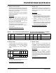
9. Module: A/D
The A/D offset is greater than the specified limit in
Table 25-24 of the Device Data Sheet. The
updated conditions and limits are shown in bold
text in Table 2.
Work around
Three work arounds exist.
1. Configure the A/D to use the V
REF+ and VREF-
pins for the voltage references. This is done by
setting the VCFG<1:0> bits (ADCON1<5:4>).
2. Perform a conversion on a known voltage
reference voltage and adjust the A/D result in
software.
3. Increase system clock speed to 40 MHz and
adjust A/D settings accordingly. Higher system
clock frequencies decrease offset error.
Date Codes that pertain to this issue:
All engineering and production devices.
TABLE 2: A/D CONVERTER CHARACTERISTICS: PIC18F2X1X/4X1X (INDUSTRIAL, EXTENDED)
PIC18LF2X1X/4X1X (INDUSTRIAL)
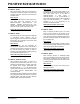
10. Module: BOR
The BOR module may reset below the minimum
operating voltage of the device when configured
for BORV1:BORV0 = 11. The updated Reset
voltage specifications are shown in bold in
Table 3.
TABLE 3: BROWN-OUT RESET VOLTAGE
Work around
Use the next higher BOR voltage setting to ensure
a low V
DD is detected above 2.0V.
Date Codes that pertain to this issue:
All engineering and production devices.
11. Module: ECCP
ECCP1 configured for auto-shutdown with
Comparator 1 corrupts the PWM duty cycle pulse.
In addition, it does not always synchronize the
pulse to the beginning of the period and the end of
the pulse can occur at any time within the period.
Work around
Use FLT0 for the auto-shutdown source.
Applications which can tolerate a shutdown
response time of several T
CYs may use the com-
parator interrupt flag to detect a shutdown event
and disable the PWM by clearing the EECPASE bit
(ECCP1AS<7>).
Date Codes that pertain to this issue:
All engineering and production devices.
Param
No.
Symbol Characteristic Min Typ Max Units Conditions
A06A E
OFF Offset Error — — <±2.0 LSb VREF = VREF+ and VREF-
A06 E
OFF Offset Error — — <±3.5 LSb VREF = VSS and VDD
Param
No.
Sym Characteristic Min Typ Max Unit
D005 V
BOR Brown-out Reset Voltage
PIC18LF2515/2610/4515/4610
BORV1:BORV0 = 11 N/A 2.05 N/A V