
Information

PIC18F2X1X/4X1X
DS80227B-page 2 © 2005 Microchip Technology Inc.
3. Module: DC Characteristics
In Section 25.3 “DC Characteristics”
(page 326), the specifications for V
IL parameters
D033B and D034 have been clarified and now
read as follows:
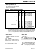
4. Module: A/D Converter Characteristics
In Table 25-24: A/D Converter Characteristics
(page 349), specification A40 has been added:
TABLE 25-24: A/D CONVERTER CHARACTERISTICS: PIC18F2X1X/4X1X (INDUSTRIAL, EXTENDED)
PIC18LF2X1X/4X1X (INDUSTRIAL)
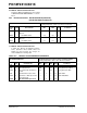
5. Module: Instruction Set
In Table 23-2: PIC18FXXXX Instruction Set
(page 261), the BTG instruction has been modified.
The changes are shown in bold text:
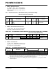
25.3 DC Characteristics: PIC18F2X1X/4X1X (Industrial, Extended)
PIC18LF2X1X/4X1X (Industrial)
DC CHARACTERISTICS
Standard Operating Conditions (unless otherwise stated)
Operating temperature -40°C ≤ T
A ≤ +85°C for industrial
Param
No.
Symbol Characteristic Min Max Units Conditions
V
IL Input Low Voltage
D033B
D034
OSC1
T13CKI
V
SS
VSS
0.3
0.3
V
V
XT, LP modes
Param
No.
Symbol Characteristic Min Typ Max Units Conditions
A40 I
AD A/D Current from VDD PIC18FXXXX — 180 — μA Average current during
conversion
PIC18LFXXXX — 90 — μA
TABLE 23-2: PIC18FXXXX INSTRUCTION SET
Mnemonic,
Operands
Description Cycles
16-Bit Instruction Word
Status
Affected
Notes
MSb LSb
BIT-ORIENTED OPERATIONS
BTG f, b, a Bit Toggle f 1 0111 bbba ffff ffff None 1, 2
Note 1: When a Port register is modified as a function of itself (e.g., MOVF PORTB, 1, 0), the value used will be
that value present on the pins themselves. For example, if the data latch is ‘1’ for a pin configured as input
and is driven low by an external device, the data will be written back with a ‘0’.
2: If this instruction is executed on the TMR0 register (and where applicable, ‘d’ = 1), the prescaler will be
cleared if assigned.