
Information


PIC18F46J11
DS80000435K-page 2 2009-2013 Microchip Technology Inc.
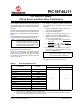
TABLE 2: SILICON ISSUE SUMMARY
Module Feature
Item
Number
Issue Summary
Affected
Revisions
(1)
A2 A4
MSSP I
2
C™
Mode
1. If a Stop condition occurs in the middle of an address
or data reception, there will be issues with the SCL
clock stream and RCEN bit.
XX
MSSP I
2
C™ Slave
Reception
2. In I
2
C™ slave reception, the module may have
problems receiving correct data.
XX
EUSART Enable/
Disable
3. If interrupts are enabled, disabling and
re-enabling the module requires a 2 TCY delay.
XX
A/D FOSC/2 Clock 4. FOSC/2 A/D Conversion mode may not meet linearity
error limits.
XX
PMP PSP/PMP 5. The data bus may not work correctly. X
Low Power
Modes
Deep Sleep 6. Wake-up events that occur during Deep Sleep entry
may not generate an event.
XX
DC Characteristics Supply
Voltage
7. Minimum operating voltage (V
DD)
Parameter F devices is 2.25V.
X
Special Features T1DIG 8. T1DIG Configuration bit is not implemented. X X
MSSP Port 1 9. When MSSP1 is in I
2
C™ mode, the RB4 and RB5
pins may have extraneous pulses.
X
A/D Band Gap
Reference
10. At high V
DD voltages, performing an A/D conversion
on Channel 15 could have issues.
XX
CTMU Constant
Current
11. V
DD voltages below the LVDSTAT threshold can
cause the constant current source to turn off.
X
A/D Converter Sample
Acquisition
12. ANx pin may output pull-up pulse during acquisition. X X
Timer1/Timer3 Async Timer
Interrupts
13. Spurious timer interrupt flag generation is possible
when writing to the timer in Async Timer mode.
XX
Note 1: Only those issues indicated in the last column apply to the current silicon revision.