
Information


© 2005 Microchip Technology Inc. DS80122K-page 7
PIC18FXX2
2. Module: Packaging (Pinout and Product
Identification)
PIC18F442 and PICF452 devices are now offered
in 44-pin, near chip-scale micro lead frame
packages (commonly known as “QFN”). This
packaging type has been added to the product line
since the latest revision of the Device Data Sheet.
The addition of this option requires the following
additions to the Device Data Sheet (DS39564B).
The referenced figures and tables follow this text.
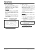
1. The “Pin Diagrams” on pages 2-3 of the Data
Sheet are amended with the addition of the
44-pin QFN pinout, shown in Figure 1.
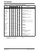
2. Table 1-3 of Section 1.0 “Overview” is
replaced with an updated version which adds a
column for QFN pin assignments. A row is also
added for previously unlisted NC pins. All new
information is indicated in bold.
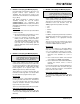
3. Section 24.1 “Package Marking Information”
is amended to include a marking template and
example for 44-pin QFN devices. These are
shown in Figure 1.
4. Section 24.2 “Package Details” is amended to
include the mechanical drawing of the 44-pin
QFN package following the existing drawings.
This is shown in Figure 2.
5. In the “PIC18FXX2 Product Identification
System” (page 329), the “Package” options are
amended to include the new line item:
ML = QFN
For the sake of completeness, it is also noted that
the package designation “MLF” is now replaced by
“QFN” in all occurrences throughout the Device
Data Sheet. “MLF” should be considered an
obsoleted term.
FIGURE 1: PINOUT DIAGRAM FOR 44-PIN QFN PACKAGE
FIGURE 1: PACKAGE MARKING TEMPLATE FOR PIC18F442/452, 44-PIN QFN
10
11
2
3
4
5
6
1
18
19
20
21
22
12
13
14
15
38
8
7
44
43
42
41
40
39
16
17
29
30
31
32
33
23
24
25
26
27
28
36
34
35
9
PIC18F442
37
RA3/AN3/VREF+
RA2/AN2/V
REF-
RA1/AN1
RA0/AN0
MCLR
/VPP
RB3/CCP2*
RB7/PGD
RB6/PGC
RB5/PGM
RB4
NC
RC6/TX/CK
RC5/SDO
RC4/SDI/SDA
RD3/PSP3
RD2/PSP2
RD1/PSP1
RD0/PSP0
RC3/SCK/SCL
RC2/CCP1
RC1/T1OSI/CCP2
RC0/T13CKI
OSC2/CLKO/RA6
OSC1/CLKI
V
SS
VSS
VDD
VDD
RE2/AN7/CS
RE1/AN6/WR
RE0/AN5/RD
RA5/AN4/SS/LVDIN
RA4/T0CKI
RC7/RX/DT
RD4/PSP4
RD5/PSP5
RD6/PSP6
RD7/PSP7
V
SS
VDD
VDD
RB0/INT0
RB1/INT1
RB2/INT2
QFN
PIC18F452
XXXXXXXXXX
44-Lead QFN
XXXXXXXXXX
XXXXXXXXXX
YYWWNNN
PIC18F442
Example
-I/ML
0510017