
Information


PIC18FXX2
DS80122K-page 4 © 2005 Microchip Technology Inc.
8. Module: Data EEPROM
When reading the data EEPROM, the contents of
the EEDATA register may be corrupted if the RD
bit (EECON1<0>) is set immediately following a
write to the address byte (EEADR). The actual
contents of the data EEPROM remain unaffected.
Work around
Do not set EEADR immediately before the
execution of a read. Write to EEADR at least one
instruction cycle before setting the RD bit. The
instruction between the write to EEADR and the
read can be any valid instruction, including a NOP.
Date Codes that pertain to this issue:
All engineering and production devices.
9. Module: MSSP (All I
2
C™ and SPI™ Modes)
The Buffer Full (BF) flag bit of the SSPSTAT
register (SSPSTAT<0>) may be inadvertently
cleared even when the SSPBUF register has not
been read. This will occur only when the following
two conditions occur simultaneously:
• The four Least Significant bits of the BSR register
are equal to 0Fh (BSR<3:0> = 1111) and
• Any instruction that contains C9h in its 8 Least
Significant bits (i.e., register file addresses,
literal data, address offsets, etc.) is executed.
Work around
All work arounds will involve setting the contents of
BSR<3:0> to some value other than 0Fh.
In addition to those proposed below, other
solutions may exist.
1. When developing or modifying code, keep
these guidelines in mind:
• Assign 12-bit addresses to all variables.
This allows the assembler to know when
Access Banking can be used.
• Do not set the BSR to point to Bank 15
(BSR = 0Fh).
• Allow the assembler to manipulate the
access bit present in most instructions.
Accessing the SFRs in Bank 15 will be done
through the Access Bank. Continue to use
the BSR to select all GPR Banks.
2. If accessing a part of Bank 15 is required and
the use of Access Banking is not possible,
consider using indirect addressing.
3. If pointing the BSR to Bank 15 is unavoidable,
review the absolute file listing. Verify that no
instructions contain C9h in the 8 Least
Significant bits while the BSR points to Bank 15
(BSR = 0Fh).
Date Codes that pertain to this issue:
All engineering and production devices.
10. Module: MSSP (SPI, Slave Mode)
In its current implementation, the SS (Slave
Select) control signal, generated by an external
master processor, may not be successfully recog-
nized by the PIC
®
microcontroller operating in
Slave Select mode (SSPM3:SSPM0 = 0100). In
particular, it has been observed that faster
transitions (those with shorter fall times) are more
likely to be missed than than slower transitions.
Work around
Insert a series resistor between the source of the
SS
signal and the corresponding SS input line of
the microcontroller. The value of the resistor is
dependent on both the application system’s
characteristics and process variations between
microcontrollers. Experimentation and thorough
testing is encouraged.
This is a recommended solution. Others may exist.
Date Codes that pertain to this issue:
All engineering and production devices.
11. Module: Core (Instruction Set)
The Decimal Adjust W register instruction, DAW,
may improperly clear the Carry bit (STATUS<0>)
when executed.
Work around
Test the Carry bit state before executing the DAW
instruction. If the Carry bit is set, increment the
next higher byte to be added using an instruction
such as INCFSZ (this instruction does not affect
any Status flags, and will not overflow a BCD
nibble). After the DAW instruction has been
executed, process the Carry bit normally (see
Example 2).
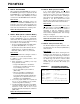
EXAMPLE 2: PROCESSING THE CARRY
BIT DURING BCD ADDITIONS
MOVLW 0x80 ; .80 (BCD)
ADDLW 0x80 ; .80 (BCD)
BTFSC STATUS,C ; test C
INCFSZ byte2 ; inc next higher LSB
DAW
BTFSC STATUS,C ; test C
INCFSZ byte2 ; inc next higher LSB
This is repeated for each DAW instruction.