
Information


© 2005 Microchip Technology Inc. DS80122K-page 13
PIC18FXX2
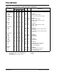
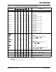
3. Module: DC Characteristics
The following parameters in Section 22.2 “DC
Characteristics” have been updated as follows:
• D032A has been changed and renamed D033
• D033 has been changed and renamed D033A
• D033B has been added
• D042A has been changed and renamed D043
• D043 has been changed and renamed D043A
• D043B has been added.
Changes are shown in bold text in the following
table.
22.2 DC Characteristics: PIC18FXX2 (Industrial, Extended)
PIC18LFXX2 (Industrial)
DC CHARACTERISTICS
Standard Operating Conditions (unless otherwise stated)
Operating temperature -40°C ≤ TA ≤ +85°C for industrial
-40°C ≤ T
A ≤ +125°C for extended
Param
No.
Symbol Characteristic Min Max Units Conditions
V
IL Input Low Voltage
I/O ports:
D030 with TTL buffer V
SS 0.15 VDD VVDD < 4.5V
D030A — 0.8 V 4.5V ≤ VDD ≤ 5.5V
D031 with Schmitt Trigger buffer
RC3 and RC4
VSS
VSS
0.2 VDD
0.3 VDD
V
V
D032 MCLR
VSS 0.2 VDD V
D033 OSC1 (HS mode) VSS 0.3 VDD V
D033A OSC1 (in RC and EC mode)
(1)
VSS 0.2 VDD V
D033B OSC1 (in XT and LP modes and
T1OSI)
VSS 0.3 V
V
IH Input High Voltage
I/O ports:
D040 with TTL buffer 0.25 VDD + 0.8V VDD VVDD < 4.5V
D040A 2.0 V
DD V4.5V ≤ VDD ≤ 5.5V
D041 with Schmitt Trigger buffer
RC3 and RC4
0.8 VDD
0.7 VDD
VDD
VDD
V
V
D042 MCLR
, OSC1 (EC mode) 0.8 VDD VDD V
D043 OSC1 (HS mode) 0.7 VDD VDD V
D043A OSC1 (RC mode)
(1)
0.9 VDD VDD V
D043B OSC1 (in XT and LP modes and
T1OSI)
1.6 V
DD V
Note 1: In RC oscillator configuration, the OSC1/CLKI pin is a Schmitt Trigger input. It is not recommended that the
PICmicro
®
device be driven with an external clock while in RC mode.
2: The leakage current on the MCLR
pin is strongly dependent on the applied voltage level. The specified
levels represent normal operating conditions. Higher leakage current may be measured at different input
voltages.
3: Negative current is defined as current sourced by the pin.
4: Parameter is characterized but not tested.