
Information

PIC18FXX2
DS80173C-page 8 © 2005 Microchip Technology Inc.
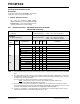
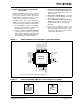
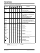
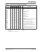
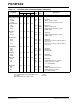
TABLE 1-3: PIC18F4X2 PINOUT I/O DESCRIPTIONS
Pin Name
Pin Number
Pin
Type
Buffer
Type
Description
DIP PLCC QFN TQFP
MCLR
/VPP
MCLR
VPP
1218 18
I
I
ST
ST
Master Clear (input) or high-voltage ICSP™
programming enable pin.
Master Clear (Reset) input. This pin is an active
low Reset to the device.
High-voltage ICSP programming enable pin.
NC — 32 — — These pins should be left unconnected.
OSC1/CLKI
OSC1
CLKI
13 14 33 30
I
I
ST
CMOS
Oscillator crystal or external clock input.
Oscillator crystal input or external clock source
input. ST buffer when configured in RC mode,
CMOS otherwise.
External clock source input. Always associated
with pin function OSC1. (See related
OSC1/CLKI, OSC2/CLKO pins.)
OSC2/CLKO/RA6
OSC2
CLKO
RA6
14 15 31
O
O
I/O
—
—
TTL
Oscillator crystal or clock output.
Oscillator crystal output. Connects to crystal
or resonator in Crystal Oscillator mode.
In RC mode, OSC2 pin outputs CLKO, which
has 1/4 the frequency of OSC1 and denotes the
instruction cycle rate.
General purpose I/O pin.
PORTA is a bidirectional I/O port.
RA0/AN0
RA0
AN0
2319 19
I/O
I
TTL
Analog
Digital I/O.
Analog input 0.
RA1/AN1
RA1
AN1
3420 20
I/O
I
TTL
Analog
Digital I/O.
Analog input 1.
RA2/AN2/V
REF-
RA2
AN2
V
REF-
4521 21
I/O
I
I
TTL
Analog
Analog
Digital I/O.
Analog input 2.
A/D Reference Voltage (Low) input.
RA3/AN3/VREF+
RA3
AN3
V
REF+
5622 22
I/O
I
I
TTL
Analog
Analog
Digital I/O.
Analog input 3.
A/D Reference Voltage (High) input.
RA4/T0CKI
RA4
T0CKI
6723 23
I/O
I
ST/OD
ST
Digital I/O. Open-drain when configured as output.
Timer0 external clock input.
RA5/AN4/SS
/LVDIN
RA5
AN4
SS
LVDIN
7824 24
I/O
I
I
I
TTL
Analog
ST
Analog
Digital I/O.
Analog input 4.
SPI™ Slave Select input.
Low-Voltage Detect input.
RA6 (See the OSC2/CLKO/RA6 pin.)
Legend: TTL = TTL compatible input CMOS = CMOS compatible input or output
ST = Schmitt Trigger input with CMOS levels I = Input
O = Output P = Power
OD = Open-Drain (no P diode to V
DD)