
Information

PIC18FXX2
DS80173C-page 4 © 2005 Microchip Technology Inc.
Clarifications/Corrections to the
Data Sheet:
In the Device Data Sheet (DS39564B), the following
clarifications and corrections should be noted.
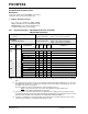
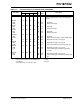
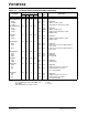
1. Module: DC Characteristics
The values for parameters, D005, D010A,
D022A and D022B, shown in Section 22.1 “DC
Characteristics” of the Device Data Sheet have
changed (modified text is shown in bold):
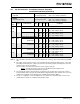
22.1 DC Characteristics: PIC18FXX2 (Industrial, Extended)
PIC18LFXX2 (Industrial)
PIC18LFXX2
(Industrial)
Standard Operating Conditions (unless otherwise stated)
Operating temperature -40°C ≤ T
A ≤ +85°C for industrial
PIC18FXX2
(Industrial, Extended)
Standard Operating Conditions (unless otherwise stated)
Operating temperature -40°C ≤ T
A ≤ +85°C for industrial
-40°C ≤ T
A ≤ +125°C for extended
Param
No.
Symbol Characteristic Min Typ Max Units Conditions
V
BOR Brown-out Reset Voltage
D005 PIC18LFXX2
BORV1:BORV0 = 11 1.96 2.06 2.16 V85°C ≥ T ≥ 25°C
BORV1:BORV0 = 10 2.64 2.78 2.92 V
BORV1:BORV0 = 01 4.11 4.33 4.55 V
BORV1:BORV0 = 00 4.41 4.64 4.87 V
D005 PIC18FXX2
BORV1:BORV0 = 1x N.A. — N.A. V Not in operating voltage range of device
BORV1:BORV0 = 01 4.16 — 4.5 V
BORV1:BORV0 = 00 4.45 — 4.83 V
D005 PIC18FXX2
BORV1:BORV0 = 1x N.A. — N.A. V Extended devices operating at 125°C
BORV1:BORV0 = 01 4.07 — 4.59 V
BORV1:BORV0 = 00 4.36 — 4.92 V
Legend: Shading of rows is to assist in readability of the table.
Note 1: This is the limit to which V
DD can be lowered in Sleep mode, or during a device Reset, without losing RAM
data.
2: The supply current is mainly a function of the operating voltage and frequency. Other factors, such as I/O
pin loading and switching rate, oscillator type, internal code execution pattern and temperature, also have
an impact on the current consumption.
The test conditions for all I
DD measurements in active operation mode are:
OSC1 = external square wave, from rail-to-rail; all I/O pins tri-stated, pulled to V
DD
MCLR
= VDD; WDT enabled/disabled as specified.
3: The power-down current in Sleep mode does not depend on the oscillator type. Power-down current is
measured with the part in Sleep mode, with all I/O pins in high-impedance state and tied to V
DD or VSS and
all features that add delta current disabled (such as WDT, Timer1 Oscillator, BOR,...).
4: For RC osc configuration, current through R
EXT is not included. The current through the resistor can be
estimated by the formula Ir = V
DD/2REXT (mA) with REXT in kΩ.