
Information

© 2005 Microchip Technology Inc. DS80173C-page 11
PIC18FXX2
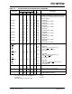
PORTD is a bidirectional I/O port, or a Parallel Slave
Port (PSP) for interfacing to a microprocessor port.
These pins have TTL input buffers when the PSP
module is enabled.
RD0/PSP0 19 21 38 38 I/O ST
TTL
Digital I/O.
Parallel Slave Port Data.
RD1/PSP1 20 22 39 39 I/O ST
TTL
Digital I/O.
Parallel Slave Port Data.
RD2/PSP2 21 23 40 40 I/O ST
TTL
Digital I/O.
Parallel Slave Port Data.
RD3/PSP3 22 24 41 41 I/O ST
TTL
Digital I/O.
Parallel Slave Port Data.
RD4/PSP4 27 30 2 2 I/O ST
TTL
Digital I/O.
Parallel Slave Port Data.
RD5/PSP5 28 31 3 3 I/O ST
TTL
Digital I/O.
Parallel Slave Port Data.
RD6/PSP6 29 32 4 4 I/O ST
TTL
Digital I/O.
Parallel Slave Port Data.
RD7/PSP7 30 33 5 5 I/O ST
TTL
Digital I/O.
Parallel Slave Port Data.
PORTE is a bidirectional I/O port.
RE0/RD
/AN5
RE0
RD
AN5
8925 25 I/O
ST
TTL
Analog
Digital I/O.
Read control for parallel slave port
(see also WR
and CS pins).
Analog input 5.
RE1/WR
/AN6
RE1
WR
AN6
91026 26 I/O
ST
TTL
Analog
Digital I/O.
Write control for parallel slave port
(see CS
and RD pins).
Analog input 6.
RE2/CS
/AN7
RE2
CS
AN7
10 11 27 27 I/O
ST
TTL
Analog
Digital I/O.
Chip Select control for parallel slave port
(see related RD
and WR).
Analog input 7.
V
SS 12,
31
13, 34 6, 30,
31
6, 29 P — Ground reference for logic and I/O pins.
V
DD 11,
32
12, 35 7, 8,
28, 29
7, 28 P — Positive supply for logic and I/O pins.
NC — 1, 17,
28
13 12, 13,
33, 34
— — These pins are not internally connected. They
should be left unconnected.
TABLE 1-3: PIC18F4X2 PINOUT I/O DESCRIPTIONS (CONTINUED)
Pin Name
Pin Number
Pin
Type
Buffer
Type
Description
DIP PLCC QFN TQFP
Legend: TTL = TTL compatible input CMOS = CMOS compatible input or output
ST = Schmitt Trigger input with CMOS levels I = Input
O = Output P = Power
OD = Open-Drain (no P diode to V
DD)