
Information

© 2005 Microchip Technology Inc. DS80173C-page 1
PIC18FXX2
The PIC18FXX2 Rev. C0 parts you have received
conform functionally to the Device Data Sheet
(DS39564B), except for the anomalies described
below.
All the issues listed here will be addressed in future
revisions of the PIC18FXX2 silicon.
The following silicon errata apply only to
PIC18FXX2 devices with these Device/Revision
IDs:
1. Module: Core (Program Memory Space)
Performing table read operations above the user
program memory space (addresses over
1FFFFFh) may yield erroneous results at the
extreme low end of the device’s rated temperature
range (-40°C).
This applies specifically to addresses above
1FFFFFh, including the user ID locations
(200000h-200007h), the configuration bytes
(300000h-30000Dh) and the device ID locations
(3FFFFEh and 3FFFFFh). User program memory
is unaffected.
Work around
Three possible work arounds are presented. Other
solutions may exist.
1. Do not perform table read operations on areas
above the user memory space at -40°C.
2. Insert NOP instructions (specifically, literal
FFFFh) around any table read instructions.
The suggested optimal number is 4 instruc-
tions before and 8 instructions after each table
read. This may vary depending upon the
particular application and should be optimized
by the user.
Date Codes that pertain to this issue:
All engineering and production devices.
2. Module: Data EEPROM
When reading the data EEPROM, the contents of
the EEDATA register may be corrupted if the RD
bit (EECON1<0>) is set immediately following a
write to the address byte (EEADR). The actual
contents of the data EEPROM remain unaffected.
Work around
Do not set EEADR immediately before the
execution of a read. Write to EEADR at least one
instruction cycle before setting the RD bit. The
instruction between the write to EEADR and the
read can be any valid instruction, including a NOP.
Date Codes that pertain to this issue:
All engineering and production devices.
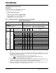
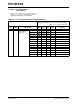
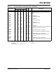
Part Number Device ID Revision ID
PIC18F242 00 0100 100 00111
PIC18F252 00 0100 000 00111
PIC18F442 00 0100 101 00111
PIC18F452 00 0100 001 00111
The Device IDs (DEVID1 and DEVID2) are located at
addresses 3FFFFEh:3FFFFFh in the device’s
configuration space. They are shown in hexadecimal
in the format “DEVID2 DEVID1”.
PIC18FXX2 Rev. C0 Silicon/Data Sheet Errata