
Information


© 2005 Microchip Technology Inc. DS80150D-page 9
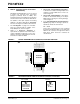
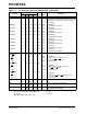
PIC18FXX2
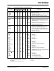
PORTC is a bidirectional I/O port.
RC0/T1OSO/T1CKI
RC0
T1OSO
T1CKI
15 16 34 32
I/O
O
I
ST
—
ST
Digital I/O.
Timer1 oscillator output.
Timer1/Timer3 external clock input.
RC1/T1OSI/CCP2
RC1
T1OSI
CCP2
16 18 35 35
I/O
I
I/O
ST
CMOS
ST
Digital I/O.
Timer1 oscillator input.
Capture2 input, Compare2 output,
PWM2 output.
RC2/CCP1
RC2
CCP1
17 19 36 36
I/O
I/O
ST
ST
Digital I/O.
Capture1 input/Compare1 output/
PWM1 output.
RC3/SCK/SCL
RC3
SCK
SCL
18 20 37 37
I/O
I/O
I/O
ST
ST
ST
Digital I/O.
Synchronous serial clock input/output for
SPI™ mode.
Synchronous serial clock input/output for
I
2
C™ mode.
RC4/SDI/SDA
RC4
SDI
SDA
23 25 42 42
I/O
I
I/O
ST
ST
ST
Digital I/O.
SPI Data In.
I
2
C Data I/O.
RC5/SDO
RC5
SDO
24 26 43 43
I/O
O
ST
—
Digital I/O.
SPI Data Out.
RC6/TX/CK
RC6
TX
CK
25 27 44 44
I/O
O
I/O
ST
—
ST
Digital I/O.
USART Asynchronous Transmit.
USART Synchronous Clock
(see related RX/DT).
RC7/RX/DT
RC7
RX
DT
26 29 1 1
I/O
I
I/O
ST
ST
ST
Digital I/O.
USART Asynchronous Receive.
USART Synchronous Data
(see related TX/CK).
TABLE 1-3: PIC18F442/452 PINOUT I/O DESCRIPTIONS (CONTINUED)
Pin Name
Pin Number
Pin
Type
Buffer
Type
Description
DIP PLCC QFN TQFP
Legend: TTL = TTL compatible input CMOS = CMOS compatible input or output
ST = Schmitt Trigger input with CMOS levels I = Input
O = Output P = Power
OD = Open Drain (no P diode to V
DD)