
Information


© 2005 Microchip Technology Inc. DS80150D-page 1
PIC18FXX2
The PIC18FXX2 Rev. B5 parts you have received con-
form functionally to the Device Data Sheet
(DS39564B), except for the anomalies described
below.
All the issues listed here will be addressed in future
revisions of the PIC18FXX2 silicon.
The following silicon errata apply only to
PIC18FXX2 devices with these Device/Revision
IDs:
1. Module: Program Memory
Data corruption may occur during a table write
operation if a peripheral interrupt also occurs. This
happens only when the interrupt enable bit (PIE or
INTCON register) for the corresponding interrupt
has also been set.
Work around
Before executing any table write instructions, dis-
able ALL peripheral interrupts. This is best done by
clearing all interrupt enable bits in the three Inter-
rupt Control registers (INTCON, INTCON2 and
INTCON3) and both Peripheral Interrupt Enable
registers (PIE1 and PIE2). After the table write is
complete, restore all INTCON and PIE registers to
their pre-instruction state.
Date Codes that pertain to this issue:
All engineering and production devices.
2. Module: Data EEPROM
When reading the data EEPROM, the contents of
the EEDATA register may become corrupted in the
second instruction cycle after the RD bit
(EECON1<0>) is set. The actual contents of the
EEPROM remains unaffected.
Work around
To ensure the integrity of the contents of EEDATA,
the register must be read in the instruction imme-
diately following the setting of the RD bit. Use the
MOVF or MOVFF instructions to do this (see
Example 1).
Additionally, all interrupts must be disabled prior to
the read instruction sequence. Interruptions of the
sequence may have the same result of altering the
contents of EEDATA.
EXAMPLE 1: SUGGESTED SEQUENCE
FOR READING EEDATA
Date Codes that pertain to this issue:
All engineering and production devices.
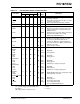
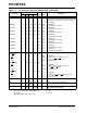
Part Number Device ID Revision ID
PIC18F242 00 0100 100 00110
PIC18F252 00 0100 000 00110
PIC18F442 00 0100 101 00110
PIC18F452 00 0100 001 00110
The Device IDs (DEVID1 and DEVID2) are located at
addresses 3FFFFEh:3FFFFFh in the device’s
configuration space. They are shown in hexadecimal
in the format “DEVID2 DEVID1”.
•
•
BCF INTCON,GIEH ;disable interrupts
;if using interrupts
BSF EECON1,RD ;start the read operation
MOVF EEDATA,W ;move the data out of
;EEDATA
BSF INTCON,GIEH ;enable interrupts
;if using interrupts
•
•
PIC18FXX2 Rev. B5 Silicon/Data Sheet Errata