
Datasheet


2010 Microchip Technology Inc. DS41303G-page 79
PIC18F2XK20/4XK20
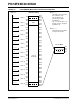
TABLE 5-2: REGISTER FILE SUMMARY (PIC18F2XK20/4XK20)
File Name Bit 7 Bit 6 Bit 5 Bit 4 Bit 3 Bit 2 Bit 1 Bit 0
Value on
POR, BOR
Details
on page:
TOSU
— — — Top-of-Stack Upper Byte (TOS<20:16>) ---0 0000 59, 66
TOSH Top-of-Stack, High Byte (TOS<15:8>) 0000 0000 59, 66
TOSL Top-of-Stack, Low Byte (TOS<7:0>) 0000 0000 59, 66
STKPTR STKFUL STKUNF
— SP4 SP3 SP2 SP1 SP0 00-0 0000 59, 67
PCLATU
— — — Holding Register for PC<20:16> ---0 0000 59, 66
PCLATH Holding Register for PC<15:8> 0000 0000 59, 66
PCL PC, Low Byte (PC<7:0>) 0000 0000 59, 66
TBLPTRU
— — bit 21 Program Memory Table Pointer Upper Byte (TBLPTR<20:16>) --00 0000 59, 92
TBLPTRH Program Memory Table Pointer, High Byte (TBLPTR<15:8>) 0000 0000 59, 92
TBLPTRL Program Memory Table Pointer, Low Byte (TBLPTR<7:0>) 0000 0000 59, 92
TABLAT Program Memory Table Latch 0000 0000 59, 92
PRODH Product Register, High Byte xxxx xxxx 59, 105
PRODL Product Register, Low Byte xxxx xxxx 59, 105
INTCON GIE/GIEH PEIE/GIEL TMR0IE INT0IE RBIE TMR0IF INT0IF RBIF 0000 000x 59, 109
INTCON2 RBPU
INTEDG0 INTEDG1 INTEDG2 —TMR0IP—RBIP1111 -1-1 59, 110
INTCON3 INT2IP INT1IP
—INT2IEINT1IE— INT2IF INT1IF 11-0 0-00 59, 111
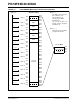
INDF0 Uses contents of FSR0 to address data memory – value of FSR0 not changed (not a physical register) N/A 59, 84
POSTINC0 Uses contents of FSR0 to address data memory – value of FSR0 post-incremented (not a physical register) N/A 59, 84
POSTDEC0 Uses contents of FSR0 to address data memory – value of FSR0 post-decremented (not a physical register) N/A 59, 84
PREINC0 Uses contents of FSR0 to address data memory – value of FSR0 pre-incremented (not a physical register) N/A 59, 84
PLUSW0 Uses contents of FSR0 to address data memory – value of FSR0 offset by W (not a physical register) – N/A 59, 84
FSR0H
— — — — Indirect Data Memory Address Pointer 0, High Byte ---- 0000 59, 84
FSR0L Indirect Data Memory Address Pointer 0, Low Byte xxxx xxxx 59, 84
WREG Working Register xxxx xxxx 59
INDF1 Uses contents of FSR1 to address data memory – value of FSR1 not changed (not a physical register) N/A 59, 84
POSTINC1 Uses contents of FSR1 to address data memory – value of FSR1 post-incremented (not a physical register) N/A 59, 84
POSTDEC1 Uses contents of FSR1 to address data memory – value of FSR1 post-decremented (not a physical register) N/A 59, 84
PREINC1 Uses contents of FSR1 to address data memory – value of FSR1 pre-incremented (not a physical register) N/A 59, 84
PLUSW1 Uses contents of FSR1 to address data memory – value of FSR1 offset by W (not a physical register) – value of N/A 59, 84
FSR1H
— — — — Indirect Data Memory Address Pointer 1, High Byte ---- 0000 60, 84
FSR1L Indirect Data Memory Address Pointer 1, Low Byte xxxx xxxx 60, 84
BSR
— — — — Bank Select Register ---- 0000 60, 71
INDF2 Uses contents of FSR2 to address data memory – value of FSR2 not changed (not a physical register) N/A 60, 84
POSTINC2 Uses contents of FSR2 to address data memory – value of FSR2 post-incremented (not a physical register) N/A 60, 84
POSTDEC2 Uses contents of FSR2 to address data memory – value of FSR2 post-decremented (not a physical register) N/A 60, 84
PREINC2 Uses contents of FSR2 to address data memory – value of FSR2 pre-incremented (not a physical register) N/A 60, 84
PLUSW2 Uses contents of FSR2 to address data memory – value of FSR2 offset by W (not a physical register) – value of N/A 60, 84
FSR2H
— — — — Indirect Data Memory Address Pointer 2, High Byte ---- 0000 60, 84
FSR2L Indirect Data Memory Address Pointer 2, Low Byte xxxx xxxx 60, 84
STATUS
— — —NOVZDCC---x xxxx 60, 82
Legend: x = unknown, u = unchanged, — = unimplemented, q = value depends on condition
Note 1: The SBOREN bit is only available when the BOREN<1:0> Configuration bits = 01; otherwise it is disabled and reads as ‘0’. See
Section 4.4 “Brown-out Reset (BOR)”.
2: These registers and/or bits are not implemented on 28-pin devices and are read as ‘0’. Reset values are shown for 40/44-pin devices;
individual unimplemented bits should be interpreted as ‘-’.
3: The PLLEN bit is only available in specific oscillator configuration; otherwise it is disabled and reads as ‘0’. See Section 2.6.2 “PLL in
HFINTOSC Modes”.
4: The RE3 bit is only available when Master Clear Reset is disabled (MCLRE Configuration bit = 0). Otherwise, RE3 reads as ‘0’. This bit is
read-only.
5: RA6/RA7 and their associated latch and direction bits are individually configured as port pins based on various primary oscillator modes.
When disabled, these bits read as ‘0’.
6: All bits of the ANSELH register initialize to ‘0’ if the PBADEN bit of CONFIG3H is ‘0’.
7: This register is only implemented in the PIC18F46K20 and PIC18F26K20 devices.