
Datasheet


2010 Microchip Technology Inc. DS41303G-page 377
PIC18F2XK20/4XK20
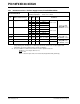
26.9 DC Characteristics: Input/Output Characteristics, PIC18F2XK20/4XK20
DC CHARACTERISTICS
Standard Operating Conditions (unless otherwise stated)
Operating temperature -40°C T
A +125°C
Param
No.
Symbol Characteristic Min Typ† Max Units Conditions
V
IL Input Low Voltage
I/O ports:
D030 with TTL buffer V
SS —0.15 VDD V
D031 with Schmitt Trigger VSS —0.2 VDD V
D032 MCLR
VSS —0.2 VDD V
D033 OSC1 VSS —0.3 VDD V HS, HSPLL modes
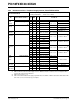
D033A
D033B
D034
OSC1
OSC1
T13CKI
V
SS
VSS
VSS
—
—
—
0.2 V
DD
0.3 VDD
0.3 VDD
V
V
V
RC, EC modes
(1)
XT, LP modes
V
IH Input High Voltage
I/O ports:
D040 with TTL buffer 0.25 VDD + 0.8V — VDD V
D041 V
IH with Schmitt Trigger: 0.8 VDD
0.9 VDD
—
—
VDD
VDD
V
V
2.4V < VDD < 3.6V
V
DD < 2.4V
D042 V
IH MCLR
0.8 VDD
0.9 VDD
—
—
VDD
VDD
V
V
2.4V < VDD < 3.6V
V
DD < 2.4V
D043 OSC1 0.7 VDD —VDD V HS, HSPLL modes
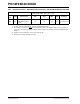
D043A
D043B
D043C
D044
OSC1
OSC1
OSC1
T13CKI
0.8 VDD
0.9 VDD
1.6
1.6
—
—
—
—
VDD
VDD
VDD
VDD
V
V
V
V
EC mode
RC mode
(1)
XT, LP modes
I
IL Input Leakage I/O and
MCLR
(2,3)
V
SS VPIN VDD,
Pin at
high-impedance
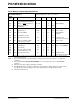
D060
D061
D062
I
IL
IIL
I/O ports
Input Leakage RA2
Input Leakage RA3
—
—
—
—
—
—
—
—
—
—
—
—
5
10
30
100
10
35
200
400
10
25
70
300
50
100
200
1000
100
250
750
2000
80
200
500
1500
nA
nA
nA
nA
nA
nA
nA
nA
nA
nA
nA
nA
+25°C
+60°C
+85°C
+125°C
+25°C
+60°C
+85°C
+125°C
+25°C
+60°C
+85°C
+125°C
Note 1: In RC oscillator configuration, the OSC1/CLKIN pin is a Schmitt Trigger input. It is not recommended that
the PIC
®
device be driven with an external clock while in RC mode.
2: The leakage current on the MCLR
pin is strongly dependent on the applied voltage level. The specified
levels represent normal operating conditions. Higher leakage current may be measured at different input
voltages.
3: Negative current is defined as current sourced by the pin.
4: Parameter is characterized but not tested.