
Datasheet


2010 Microchip Technology Inc. DS41303G-page 273
PIC18F2XK20/4XK20
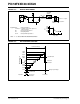
REGISTER 19-3: ADCON2: A/D CONTROL REGISTER 2
R/W-0 U-0 R/W-0 R/W-0 R/W-0 R/W-0 R/W-0 R/W-0
ADFM — ACQT2 ACQT1 ACQT0 ADCS2 ADCS1 ADCS0
bit 7 bit 0
Legend:
R = Readable bit W = Writable bit U = Unimplemented bit, read as ‘0’
-n = Value at POR ‘1’ = Bit is set ‘0’ = Bit is cleared x = Bit is unknown
bit 7 ADFM: A/D Conversion Result Format Select bit
1 = Right justified
0 = Left justified
bit 6 Unimplemented: Read as ‘0’
bit 5-3 ACQT<2:0>: A/D Acquisition time select bits. Acquisition time is the duration that the A/D charge hold-
ing capacitor remains connected to A/D channel from the instant the GO/DONE bit is set until conver-
sions begins.
000 = 0
(1)
001 = 2 TAD
010 = 4 TAD
011 = 6 TAD
100 = 8 TAD
101 = 12 TAD
110 = 16 TAD
111 = 20 TAD
bit 2-0 ADCS<2:0>: A/D Conversion Clock Select bits
000 = FOSC/2
001 = F
OSC/8
010 = F
OSC/32
011 = F
RC
(1)
(clock derived from a dedicated internal oscillator = 600 kHz nominal)
100 = F
OSC/4
101 = F
OSC/16
110 = F
OSC/64
111 = F
RC
(1)
(clock derived from a dedicated internal oscillator = 600 kHz nominal)
Note 1: When the A/D clock source is selected as F
RC then the start of conversion is delayed by one instruction
cycle after the GO/DONE bit is set to allow the SLEEP instruction to be executed.