
Datasheet


PIC18F2XK20/4XK20
DS41303G-page 238 2010 Microchip Technology Inc.
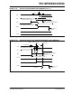
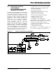
FIGURE 18-2: EUSART RECEIVE BLOCK DIAGRAM
The operation of the EUSART module is controlled
through three registers:
• Transmit Status and Control (TXSTA)
• Receive Status and Control (RCSTA)
• Baud Rate Control (BAUDCON)
These registers are detailed in Register 18-1,
Register 18-2 and Register 18-3, respectively.
For all modes of EUSART operation, the TRIS control
bits corresponding to the RX/DT and TX/CK pins should
be set to ‘1’. The EUSART control will automatically
reconfigure the pin from input to output, as needed.
When the receiver or transmitter section is not enabled
then the corresponding RX or TX pin may be used for
general purpose input and output.
RX/DT pin
Pin Buffer
and Control
Data
Recovery
CREN OERR
FERR
RSR Register
MSb
LSb
RX9D
RCREG Register
FIFO
Interrupt
RCIF
RCIE
Data Bus
8
Stop
START
(8) 7 1 0
RX9
• • •
SPBRGSPBRGH
BRG16
RCIDL
FOSC
÷ n
n
+ 1
Multiplier x4 x16 x64
SYNC 1X00 0
BRGH X110 0
BRG16 X101 0
Baud Rate Generator