
Datasheet


2010 Microchip Technology Inc. DS41303G-page 123
PIC18F2XK20/4XK20
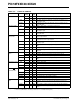
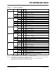
TABLE 10-2: SUMMARY OF REGISTERS ASSOCIATED WITH PORTA
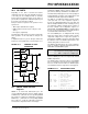
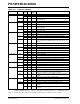
OSC1/CLKIN/RA7 RA7 0 O DIG LATA<7> data output. Disabled in external oscillator modes.
1 I TTL PORTA<7> data input. Disabled in external oscillator modes.
OSC1 x I ANA Main oscillator input connection.
CLKIN x I ANA Main clock input connection.
Name Bit 7 Bit 6 Bit 5 Bit 4 Bit 3 Bit 2 Bit 1 Bit 0
Reset
Values
on page
PORTA RA7
(1)
RA6
(1)
RA5 RA4 RA3 RA2 RA1 RA0 62
LATA LATA7
(1)
LATA6
(1)
PORTA Data Latch Register (Read and Write to Data Latch) 62
TRISA TRISA7
(1)
TRISA6
(1)
PORTA Data Direction Control Register 62
ANSEL
ANS7
(2)
ANS6
(2)
ANS5
(2)
ANS4 ANS3 ANS2 ANS1 ANS0 62
SLRCON — — — SLRE
(2)
SLRD
(2)
SLRC SLRB SLRA 63
CM1CON0 C1ON C1OUT C1OE C1POL C1SP C1R C1CH1 C1CH0 62
CM2CON0
C2ON C2OUT C2OE C2POL C2SP C2R C2CH1 C2CH0 62
CVRCON CVREN CVROE CVRR CVRSS CVR3 CVR2 CVR1 CVR0 61
Legend: — = unimplemented, read as ‘0’. Shaded cells are not used by PORTA.
Note 1: RA<7:6> and their associated latch and data direction bits are enabled as I/O pins based on oscillator
configuration; otherwise, they are read as ‘0’.
2: Not implemented on PIC18F2XK20 devices.
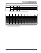
TABLE 10-1: PORTA I/O SUMMARY (CONTINUED)
Pin Function
TRIS
Setting
I/O
I/O
Type
Description
Legend: DIG = Digital level output; TTL = TTL input buffer; ST = Schmitt Trigger input buffer; ANA = Analog level input/output;
x = Don’t care (TRIS bit does not affect port direction or is overridden for this option).