
Datasheet


PIC18F2XK20/4XK20
DS41303G-page 402 2010 Microchip Technology Inc.
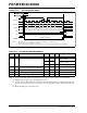
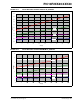
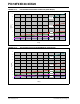
FIGURE 26-22: A/D CONVERSION TIMING
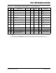
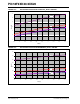
TABLE 26-25: A/D CONVERSION REQUIREMENTS
131
130
132
BSF ADCON0, GO
Q4
A/D CLK
A/D DATA
ADRES
ADIF
GO
SAMPLE
OLD_DATA
SAMPLING STOPPED
DONE
NEW_DATA
(Note 2)
987 21 0
Note 1: If the A/D clock source is selected as RC, a time of T
CY is added before the A/D clock starts.
This allows the SLEEP instruction to be executed.
2: This is a minimal RC delay (typically 100 ns), which also disconnects the holding capacitor from the analog input.
.. .
. . .
TCY
Param
No.
Symbol Characteristic Min Max Units Conditions
130 T
AD A/D Clock Period 0.7 25.0
(1)
sTOSC based,
-40C to +85C
0.7 4.0
(1)
sTOSC based,
+85C to +125C
1.0 4.0 s FRC mode, V
DD2.0V
131 TCNV Conversion Time
(not including acquisition time) (Note 2)
12 12 TAD
132 TACQ Acquisition Time (Note 3) 1.4 — sVDD = 3V, Rs = 50
135 TSWC Switching Time from Convert Sample — (Note 4)
136 T
DIS Discharge Time 2 2 TAD
Legend: TBD = To Be Determined
Note 1: The time of the A/D clock period is dependent on the device frequency and the T
AD clock divider.
2: ADRES register may be read on the following TCY cycle.
3: The time for the holding capacitor to acquire the “New” input voltage when the voltage changes full scale
after the conversion (V
DD to VSS or VSS to VDD). The source impedance (RS) on the input channels is 50
.
4: On the following cycle of the device clock.