
Datasheet


2010 Microchip Technology Inc. DS41303G-page 401
PIC18F2XK20/4XK20
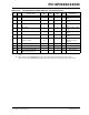
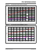
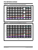
TABLE 26-24: A/D CONVERTER CHARACTERISTICS: PIC18F2XK20/4XK20
Param
No.
Symbol Characteristic Min Typ Max Units Conditions
A01 N
R Resolution — — 10 bits -40°C to +85°C, VREF
2.0V
A03 E
IL Integral Linearity Error — ±0.5 ±1 LSb -40°C to +85°C, VREF
2.0V
A04 E
DL Differential Linearity Error — ±0.4 ±1 LSb -40°C to +85°C, VREF
2.0V
A06 E
OFF Offset Error — 0.4 ±2 LSb -40°C to +85°C, VREF
2.0V
A07 E
GN Gain Error — 0.3 ±2 LSb -40°C to +85°C, VREF
2.0V
A08 E
TOTL Total Error — 1 ±3 LSb -40°C to +85°C, VREF
2.0V
A20 V
REF Reference Voltage Range
(V
REFH – VREFL)
1.8
2.0
—
—
—
—
V
V
A
Bsolute Minimum
Minimum for 1LSb
Accuracy
A21 VREFH Reference Voltage High VDD/2 — VDD + 0.3 V
A22 VREFL Reference Voltage Low VSS – 0.3V — VDD/2 V
A25 V
AIN Analog Input Voltage VREFL —VREFH V
A30 ZAIN Recommended Impedance of
Analog Voltage Source
—— 3k -40°C to +85°C
Note 1: The A/D conversion result never decreases with an increase in the input voltage and has no missing
codes.
2: VREFH current is from RA3/AN3/VREF+ pin or VDD, whichever is selected as the VREFH source.
V
REFL current is from RA2/AN2/VREF-/CVREF pin or VSS, whichever is selected as the VREFL source.