
Datasheet


2010 Microchip Technology Inc. DS41303G-page 379
PIC18F2XK20/4XK20
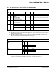
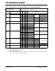
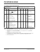
VOL Output Low Voltage
D080 I/O ports — — 0.6 V I
OL = 8.5 mA, VDD
= 3.0V,
-40C to +85C
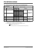
D083 OSC2/CLKOUT
(RC, RCIO, EC, ECIO
modes)
——0.6VI
OL = 1.6 mA, VDD
= 3.0V,
-40C to +85C
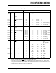
V
OH Output High Voltage
(3)
D090 I/O ports VDD – 0.7 — — V IOH = -3.0 mA, VDD
= 3.0V,
-40C to +85C
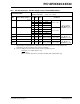
D092 OSC2/CLKOUT
(RC, RCIO, EC, ECIO
modes)
V
DD – 0.7 — — V IOH = -1.3 mA, VDD
= 3.0V,
-40C to +85C
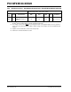
Capacitive Loading
Specs
on Output Pins
D100
(4)
COSC2 OSC2 pin
—
— 15 pF In XT, HS and LP
modes when exter-
nal clock is used to
drive OSC1
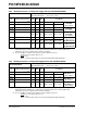
D101 C
IO All I/O pins and OSC2
(in RC mode)
— — 50 pF To meet the AC
Timing
Specifications
D102 CB SCL, SDA — — 400 pF I
2
C™ Specification
26.9 DC Characteristics: Input/Output Characteristics, PIC18F2XK20/4XK20 (Continued)
DC CHARACTERISTICS
Standard Operating Conditions (unless otherwise stated)
Operating temperature -40°C T
A +125°C
Param
No.
Symbol Characteristic Min
Typ† Max Units Conditions
Note 1: In RC oscillator configuration, the OSC1/CLKIN pin is a Schmitt Trigger input. It is not recommended that
the PIC
®
device be driven with an external clock while in RC mode.
2: The leakage current on the MCLR
pin is strongly dependent on the applied voltage level. The specified
levels represent normal operating conditions. Higher leakage current may be measured at different input
voltages.
3: Negative current is defined as current sourced by the pin.
4: Parameter is characterized but not tested.