
Datasheet

PIC18F2XK20/4XK20
DS41303G-page 350 2010 Microchip Technology Inc.
SLEEP Enter Sleep mode
Syntax: SLEEP
Operands: None
Operation: 00h WDT,
0 WDT postscaler,
1 TO
,
0 PD
Status Affected: TO, PD
Encoding: 0000 0000 0000 0011
Description: The Power-down Status bit (PD
) is
cleared. The Time-out Status bit (TO
)
is set. Watchdog Timer and its
postscaler are cleared.
The processor is put into Sleep mode
with the oscillator stopped.
Words: 1
Cycles: 1
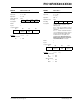
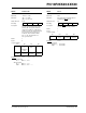
Q Cycle Activity:
Q1 Q2 Q3 Q4
Decode No
operation
Process
Data
Go to
Sleep
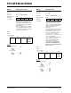
Example
: SLEEP
Before Instruction
TO
=?
PD
=?
After Instruction
TO
=1 †
PD
=0
† If WDT causes wake-up, this bit is cleared.
SUBFWB Subtract f from W with borrow
Syntax: SUBFWB f {,d {,a}}
Operands: 0 f 255
d [0,1]
a [0,1]
Operation: (W) – (f) – (C
) dest
Status Affected: N, OV, C, DC, Z
Encoding: 0101 01da ffff ffff
Description: Subtract register ‘f’ and CARRY flag
(borrow) from W (2’s complement
method). If ‘d’ is ‘0’, the result is stored
in W. If ‘d’ is ‘1’, the result is stored in
register ‘f’ (default).
If ‘a’ is ‘0’, the Access Bank is
selected. If ‘a’ is ‘1’, the BSR is used
to select the GPR bank.
If ‘a’ is ‘0’ and the extended instruction
set is enabled, this instruction
operates in Indexed Literal Offset
Addressing mode whenever
f 95 (5Fh). See Section 24.2.3
“Byte-Oriented and Bit-Oriented
Instructions in Indexed Literal Offset
Mode” for details.
Words: 1
Cycles: 1
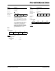
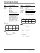
Q Cycle Activity:
Q1 Q2 Q3 Q4
Decode Read
register ‘f’
Process
Data
Write to
destination
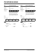
Example 1
: SUBFWB REG, 1, 0
Before Instruction
REG = 3
W=2
C=1
After Instruction
REG = FF
W=2
C=0
Z=0
N = 1 ; result is negative
Example 2
: SUBFWB REG, 0, 0
Before Instruction
REG = 2
W=5
C=1
After Instruction
REG = 2
W=3
C=1
Z=0
N = 0 ; result is positive
Example 3
: SUBFWB REG, 1, 0
Before Instruction
REG = 1
W=2
C=0
After Instruction
REG = 0
W=2
C=1
Z = 1 ; result is zero
N=0