
Datasheet


2010 Microchip Technology Inc. DS41303G-page 203
PIC18F2XK20/4XK20
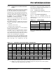
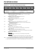
REGISTER 17-3: SSPADD: MSSP ADDRESS AND BAUD RATE REGISTER (I
2
C MODE)
R/W-0 R/W-0 R/W-0 R/W-0 R/W-0 R/W-0 R/W-0 R/W-0
ADD7 ADD6 ADD5 ADD4 ADD3 ADD2 ADD1 ADD0
bit 7 bit 0
Legend:
R = Readable bit W = Writable bit U = Unimplemented bit, read as ‘0’
-n = Value at POR ‘1’ = Bit is set ‘0’ = Bit is cleared x = Bit is unknown
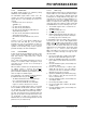
Master mode
bit 7-0 ADD<7:0>: Baud Rate Clock Divider bits
SCL pin clock period = ((ADD<7:0> + 1) *4)/F
OSC
10-Bit Slave mode: Most significant address byte
bit 7-3 Not used: Unused for most significant address byte. Bit state of this register is a don’t care. Bit pattern
sent by master is fixed by I
2
C specification and must be equal to ‘11110’. However, those bits are
compared by hardware and are not affected by the value in this register.
bit 2-1 ADD<9:8>: Two most significant bits of 10-bit address
bit 0 Not used: Unused in this mode. Bit state is a “don’t care”.
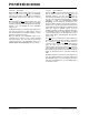
10-Bit Slave mode: Least significant address byte
bit 7-0 ADD<7:0>: Eight least significant bits of 10-bit address
7-Bit Slave mode
bit 7-1 ADD<7:1>: 7-bit address
bit 0 Not used: Unused in this mode. Bit state is a “don’t care”.