
Datasheet


2010 Microchip Technology Inc. DS41303G-page 125
PIC18F2XK20/4XK20
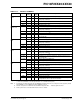
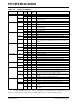
TABLE 10-3: PORTB I/O SUMMARY
Pin Function
TRIS
Setting
I/O
I/O
Type
Description
RB0/INT0/FLT0/
AN12
RB0 0 O DIG LATB<0> data output; not affected by analog input.
1 I TTL PORTB<0> data input; Programmable weak pull-up. Disabled when
analog input enabled.
(1)
INT0 1 I ST External interrupt 0 input.
FLT0 1 I ST Enhanced PWM Fault input (ECCP1 module); enabled by software.
AN12 1 I ANA A/D input channel 12.
(1)
RB1/INT1/AN10/
C12IN3-/P1C
RB1 0 O DIG LATB<1> data output; not affected by analog input.
1 I TTL PORTB<1> data input; Programmable weak pull-up. Disabled when
analog input enabled.
(1)
INT1 1 I ST External Interrupt 1 input.
AN10 1 I ANA ADC input channel 10.
(1)
C12IN3- 1 I ANA Comparators C1 and C2 inverting input, channel 3. Analog select is
shared with ADC.
P1C 0 O DIG ECCP PWM output (28-pin devices only).
RB2/INT2/AN8/
P1B
RB2 0 O DIG LATB<2> data output; not affected by analog input.
1 I TTL PORTB<2> data input; Programmable weak pull-up. Disabled when
analog input enabled.
(1)
INT2 1 I ST External interrupt 2 input.
AN8 1 I ANA ADC input channel 8.
(1)
P1B 0 O DIG ECCP PWM output (28-pin devices only).
RB3/AN9/C12IN2-/
CCP2
RB3 0 O DIG LATB<3> data output; not affected by analog input.
1 I TTL PORTB<3> data input; Programmable weak pull-up. Disabled when
analog input enabled.
(1)
AN9 1 I ANA ADC input channel 9.
(1)
C12IN2- 1 I ANA Comparators C1 and C2 inverting input, channel 2. Analog select is
shared with ADC.
CCP2
(2)
0 O DIG CCP2 compare and PWM output.
1 I ST CCP2 capture input
RB4/KBI0/AN11/
P1D
RB4 0 O DIG LATB<4> data output; not affected by analog input.
1 I TTL PORTB<4> data input; Programmable weak pull-up. Disabled when
analog input enabled.
(1)
KBI0 1 I TTL Interrupt-on-pin change.
AN11 1 I ANA ADC input channel 11.
(1)
P1D 0 O DIG ECCP PWM output (28-pin devices only).
RB5/KBI1/PGM RB5 0 O DIG LATB<5> data output.
1 I TTL PORTB<5> data input; Programmable weak pull-up.
KBI1 1 I TTL Interrupt-on-pin change.
PGM x I ST Single-Supply Programming mode entry (ICSP™). Enabled by LVP
Configuration bit; all other pin functions disabled.
Legend: DIG = Digital level output; TTL = TTL input buffer; ST = Schmitt Trigger input buffer; ANA = Analog level input/output;
x = Don’t care (TRIS bit does not affect port direction or is overridden for this option).
Note 1: Configuration on POR is determined by the PBADEN Configuration bit. Pins are configured as analog inputs by default
when PBADEN is set and digital inputs when PBADEN is cleared.
2: Alternate assignment for CCP2 when the CCP2MX Configuration bit is ‘0’. Default assignment is RC1.
3: All other pin functions are disabled when ICSP or ICD are enabled.