
Information

PIC18F2331/2431/4331/4431
DS80239A-page 8 © 2005 Microchip Technology Inc.
• A new column with pin number information for
the 28-pin QFN package has been added to
Table 1-2 (pages 12-14). New information is
shown in bold text.
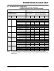
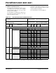
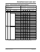
TABLE 1-2: PIC18F2331/2431 PINOUT I/O DESCRIPTIONS
Pin Name
Pin
Number
Pin
Type
Buffer
Type
Description
DIP,
SOIC
QFN
MCLR
/VPP/RE3
MCLR
VPP
RE3
1 26
I
P
I
ST
ST
Master Clear (input) or programming voltage (input).
Master Clear (Reset) input. This pin is an active-low
Reset to the device.
High-voltage ICSP programming enable pin.
Digital input. Available only when MCLR
is disabled.
OSC1/CLKI/RA7
OSC1
CLKI
RA7
9 6
I
I
I/O
ST
CMOS
TTL
Oscillator crystal or external clock input.
Oscillator crystal input or external clock source input.
ST buffer when configured in RC mode, CMOS otherwise.
External clock source input. Always associated with pin
function OSC1. (See related OSC1/CLKI, OSC2/CLKO pins.)
General purpose I/O pin.
OSC2/CLKO/RA6
OSC2
CLKO
RA6
10 7
O
O
I/O
—
—
TTL
Oscillator crystal or clock output.
Oscillator crystal output. Connects to crystal or resonator
in Crystal Oscillator mode.
In RC mode, OSC2 pin outputs CLKO, which has 1/4 the
frequency of OSC1 and denotes the instruction cycle rate.
General purpose I/O pin.
PORTA is a bidirectional I/O port.
RA0/AN0
RA0
AN0
2 27
I/O
I
TTL
Analog
Digital I/O.
Analog input 0.
RA1/AN1
RA1
AN1
3 28
I/O
I
TTL
Analog
Digital I/O.
Analog input 1.
RA2/AN2/V
REF-/CAP1/INDX
RA2
AN2
V
REF-
CAP1
INDX
4 1
I/O
I
I
I
I
TTL
Analog
Analog
ST
ST
Digital I/O.
Analog input 2.
A/D reference voltage (Low) input.
Input capture pin 1.
Quadrature Encoder Interface index input pin.
RA3/AN3/VREF+/CAP2/QEA
RA3
AN3
V
REF+
CAP2
QEA
5 2
I/O
I
I
I
I
TTL
Analog
Analog
ST
ST
Digital I/O.
Analog input 3.
A/D reference voltage (High) input.
Input capture pin 2.
Quadrature Encoder Interface channel A input pin.
RA4/AN4/CAP3/QEB
RA4
AN4
CAP3
QEB
6 3
I/O
I
I
I
TTL
Analog
ST
ST
Digital I/O.
Analog input 4.
Input capture pin 3.
Quadrature Encoder Interface channel B input pin.
Legend: TTL = TTL compatible input CMOS = CMOS compatible input or output
ST = Schmitt Trigger input with CMOS levels I = Input
O = Output P = Power
OD = Open-Drain (no diode to V
DD)