
Information

PIC18F2331/2431/4331/4431
DS80239A-page 10 © 2005 Microchip Technology Inc.
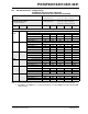
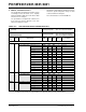
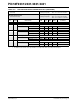
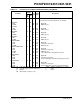
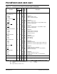
PORTC is a bidirectional I/O port.
RC0/T1OSO/T1CKI
RC0
T1OSO
T1CKI
11 8
I/O
O
I
ST
—
ST
Digital I/O.
Timer1 oscillator output.
Timer1 external clock input.
RC1/T1OSI/CCP2/FLTA
RC1
T1OSI
CCP2
FLTA
12 9
I/O
I
I/O
I
ST
CMOS
ST
ST
Digital I/O.
Timer1 oscillator input.
Capture 2 input, Compare 2 output, PWM 2 output.
Fault interrupt input pin.
RC2/CCP1/FLTB
RC2
CCP1
FLTB
13 10
I/O
I/O
I
ST
ST
ST
Digital I/O.
Capture 1 input/Compare 1 output/PWM 1 output.
Fault interrupt input pin.
RC3/T0CKI/T5CKI/INT0
RC3
T0CKI
T5CKI
INT0
14 11
I/O
I
I
I
ST
ST
ST
ST
Digital I/O.
Timer0 alternate clock input.
Timer5 alternate clock input.
External interrupt 0.
RC4/INT1/SDI/SDA
RC4
INT1
SDI
SDA
15 12
I/O
I
I
I/O
ST
ST
ST
ST
Digital I/O.
External interrupt 1.
SPI™ data in.
I
2
C™ data I/O.
RC5/INT2/SCK/SCL
RC5
INT2
SCK
SCL
16 13
I/O
I
I/O
I/O
ST
ST
ST
ST
Digital I/O.
External interrupt 2.
Synchronous serial clock input/output for SPI mode.
Synchronous serial clock input/output for I
2
C mode.
RC6/TX/CK/SS
RC6
TX
CK
SS
17 14
I/O
O
I/O
I
ST
—
ST
TTL
Digital I/O.
USART asynchronous transmit.
USART synchronous clock (see related RX/DT).
SPI slave select input.
RC7/RX/DT/SDO
RC7
RX
DT
SDO
18 15
I/O
I
I/O
O
ST
ST
ST
—
Digital I/O.
USART asynchronous receive.
USART synchronous data (see related TX/CK).
SPI data out.
V
SS 8, 19 5,
16
P — Ground reference for logic and I/O pins.
V
DD 7, 20 4,
17
P — Positive supply for logic and I/O pins.
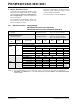
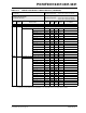
TABLE 1-2: PIC18F2331/2431 PINOUT I/O DESCRIPTIONS (CONTINUED)
Pin Name
Pin
Number
Pin
Type
Buffer
Type
Description
DIP,
SOIC
QFN
Legend: TTL = TTL compatible input CMOS = CMOS compatible input or output
ST = Schmitt Trigger input with CMOS levels I = Input
O = Output P = Power
OD = Open-Drain (no diode to V
DD)